- 您现在的位置:买卖IC网 > PDF目录18536 > NTD3055L170-1G (ON Semiconductor)MOSFET N-CH 60V 9A IPAK PDF资料下载
参数资料
| 型号: | NTD3055L170-1G |
| 厂商: | ON Semiconductor |
| 文件页数: | 2/8页 |
| 文件大小: | 0K |
| 描述: | MOSFET N-CH 60V 9A IPAK |
| 产品变化通告: | Product Obsolescence 21/Jan/2010 |
| 标准包装: | 75 |
| FET 型: | MOSFET N 通道,金属氧化物 |
| FET 特点: | 逻辑电平门 |
| 漏极至源极电压(Vdss): | 60V |
| 电流 - 连续漏极(Id) @ 25° C: | 9A |
| 开态Rds(最大)@ Id, Vgs @ 25° C: | 170 毫欧 @ 4.5A,5V |
| Id 时的 Vgs(th)(最大): | 2V @ 250µA |
| 闸电荷(Qg) @ Vgs: | 10nC @ 5V |
| 输入电容 (Ciss) @ Vds: | 275pF @ 25V |
| 功率 - 最大: | 1.5W |
| 安装类型: | 通孔 |
| 封装/外壳: | TO-251-3 短引线,IPak,TO-251AA |
| 供应商设备封装: | I-Pak |
| 包装: | 管件 |
�� �
�
�NTD3055L170,� NVD3055L170�
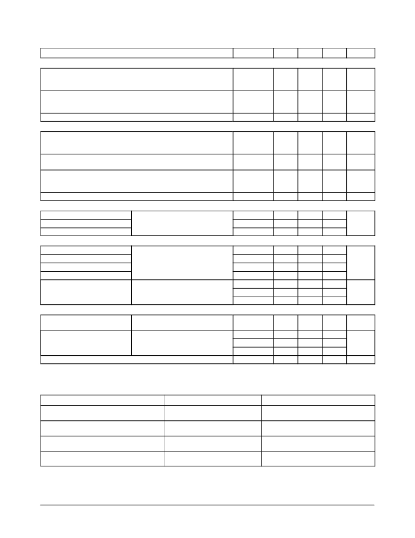
�ELECTRICAL� CHARACTERISTICS� (T� J� =� 25� °� C� unless� otherwise� noted)�
�Characteristic�
�Symbol�
�Min�
�Typ�
�Max�
�Unit�
�OFF� CHARACTERISTICS�
�Drain� ?� to� ?� Source� Breakdown� Voltage� (Note� 3)�
�(V� GS� =� 0� Vdc,� I� D� =� 250� m� Adc)�
�Temperature� Coefficient� (Positive)�
�Zero� Gate� Voltage� Drain� Current�
�(V� DS� =� 60� Vdc,� V� GS� =� 0� Vdc)�
�(V� DS� =� 60� Vdc,� V� GS� =� 0� Vdc,� T� J� =� 150� °� C)�
�Gate� ?� Body� Leakage� Current� (V� GS� =� ±� 15� Vdc,� V� DS� =� 0� Vdc)�
�V� (BR)DSS�
�I� DSS�
�I� GSS�
�60�
�?�
�?�
�?�
�?�
�?�
�53.6�
�?�
�?�
�?�
�?�
�?�
�1.0�
�10�
�±� 100�
�Vdc�
�mV/� °� C�
�m� Adc�
�nAdc�
�ON� CHARACTERISTICS� (Note� 3)�
�Gate� Threshold� Voltage� (Note� 3)�
�(V� DS� =� V� GS� ,� I� D� =� 250� m� Adc)�
�Threshold� Temperature� Coefficient� (Negative)�
�Static� Drain� ?� to� ?� Source� On� ?� Resistance� (Note� 3)�
�(V� GS� =� 5.0� Vdc,� I� D� =� 4.5� Adc)�
�Static� Drain� ?� to� ?� Source� On� ?� Voltage� (Note� 3)�
�(V� GS� =� 5.0� Vdc,� I� D� =� 9.0� Adc)�
�(V� GS� =� 5.0� Vdc,� I� D� =� 4.5� Adc,� T� J� =� 150� °� C)�
�Forward� Transconductance� (Note� 3)� (V� DS� =� 8.0� Vdc,� I� D� =� 6.0� Adc)�
�V� GS(th)�
�R� DS(on)�
�V� DS(on)�
�g� FS�
�1.0�
�?�
�?�
�?�
�?�
�?�
�1.7�
�4.2�
�153�
�1.8�
�1.3�
�7.3�
�2.0�
�?�
�170�
�2.1�
�?�
�?�
�Vdc�
�mV/� °� C�
�m� W�
�Vdc�
�mhos�
�DYNAMIC� CHARACTERISTICS�
�Input� Capacitance�
�Output� Capacitance�
�Transfer� Capacitance�
�(V� DS� =� 25� Vdc,� V� GS� =� 0� Vdc,�
�f� =� 1.0� MHz)�
�C� iss�
�C� oss�
�C� rss�
�?�
�?�
�?�
�195�
�70�
�29�
�275�
�100�
�42�
�pF�
�SWITCHING� CHARACTERISTICS� (Note� 4)�
�Turn� ?� On� Delay� Time�
�Rise� Time�
�Turn� ?� Off� Delay� Time�
�Fall� Time�
�Gate� Charge�
�(V� DD� =� 30� Vdc,� I� D� =� 9.0� Adc,�
�V� GS� =� 5.0� Vdc,�
�R� G� =� 9.1� W� )� (Note� 3)�
�(V� DS� =� 48� Vdc,� I� D� =� 9.0� Adc,�
�V� GS� =� 5.0� Vdc)� (Note� 3)�
�t� d(on)�
�t� r�
�t� d(off)�
�t� f�
�Q� T�
�Q� 1�
�Q� 2�
�?�
�?�
�?�
�?�
�?�
�?�
�?�
�9.7�
�69�
�10�
�38�
�4.7�
�1.4�
�2.9�
�20�
�150�
�20�
�80�
�10�
�?�
�?�
�ns�
�nC�
�SOURCE� ?� DRAIN� DIODE� CHARACTERISTICS�
�Forward� On� ?� Voltage�
�Reverse� Recovery� Time�
�Reverse� Recovery� Stored� Charge�
�(I� S� =� 9.0� Adc,� V� GS� =� 0� Vdc)� (Note� 3)�
�(I� S� = 9.0 Adc, V� GS� = 0 Vdc, T� J� = 150� °� C)�
�(I� S� =� 9.0� Adc,� V� GS� =� 0� Vdc,�
�dI� S� /dt� =� 100� A/� m� s)� (Note� 3)�
�V� SD�
�t� rr�
�t� a�
�t� b�
�Q� RR�
�?�
�?�
�?�
�?�
�?�
�?�
�0.98�
�0.85�
�29.8�
�17.6�
�12.2�
�0.031�
�1.25�
�?�
�?�
�?�
�?�
�?�
�Vdc�
�ns�
�m� C�
�3.� Pulse� Test:� Pulse� Width� ≤� 300� m� s,� Duty� Cycle� ≤� 2%.�
�4.� Switching� characteristics� are� independent� of� operating� junction� temperatures.�
�ORDERING� INFORMATION�
�NTD3055L170G�
�NTD3055L170� ?� 1G�
�NTD3055L170T4G�
�NVD3055L170T4G*�
�Device�
�Package�
�DPAK�
�(Pb� ?� Free)�
�DPAK� ?� 3�
�(Pb� ?� Free)�
�DPAK�
�(Pb� ?� Free)�
�DPAK�
�(Pb� ?� Free)�
�Shipping� ?�
�75� Units� /� Rail�
�75� Units� /� Rail�
�2500� /� Tape� &� Reel�
�2500� /� Tape� &� Reel�
�?For� information� on� tape� and� reel� specifications,� including� part� orientation� and� tape� sizes,� please� refer� to� our� Tape� and� Reel� Packaging�
�Specifications� Brochure,� BRD8011/D.�
�*NVD� Prefix� for� Automotive� and� Other� Applications� Requiring� Unique� Site� and� Control� Change� Requirements;� AEC� ?� Q101� Qualified� and� PPAP�
�Capable�
�http://onsemi.com�
�2�
�相关PDF资料 |
PDF描述 |
|---|---|
| ABM3C-12.288MHZ-D4Y-T | CRYSTAL 12.288 MHZ 18PF SMD |
| NTD3055-150G | MOSFET N-CH 60V 9A DPAK |
| ASEMPC-12.000MHZ-T3 | OSC 12.000 MHZ CMOS MEMS SMD |
| ASEMPC-11.0592MHZ-T3 | OSC 11.0592 MHZ CMOS MEMS SMD |
| NTD3055L170 | MOSFET N-CH 60V 9A DPAK |
相关代理商/技术参数 |
参数描述 |
|---|---|
| NTD3055L170G | 功能描述:MOSFET 60V 9A N-Channel RoHS:否 制造商:STMicroelectronics 晶体管极性:N-Channel 汲极/源极击穿电压:650 V 闸/源击穿电压:25 V 漏极连续电流:130 A 电阻汲极/源极 RDS(导通):0.014 Ohms 配置:Single 最大工作温度: 安装风格:Through Hole 封装 / 箱体:Max247 封装:Tube |
| NTD3055L170T4 | 功能描述:MOSFET 60V 9A N-Channel RoHS:否 制造商:STMicroelectronics 晶体管极性:N-Channel 汲极/源极击穿电压:650 V 闸/源击穿电压:25 V 漏极连续电流:130 A 电阻汲极/源极 RDS(导通):0.014 Ohms 配置:Single 最大工作温度: 安装风格:Through Hole 封装 / 箱体:Max247 封装:Tube |
| NTD3055L170T4G | 功能描述:MOSFET 60V 9A N-Channel RoHS:否 制造商:STMicroelectronics 晶体管极性:N-Channel 汲极/源极击穿电压:650 V 闸/源击穿电压:25 V 漏极连续电流:130 A 电阻汲极/源极 RDS(导通):0.014 Ohms 配置:Single 最大工作温度: 安装风格:Through Hole 封装 / 箱体:Max247 封装:Tube |
| NTD3055L170T4H | 制造商:ON Semiconductor 功能描述: |
| NTD30N02 | 制造商:ON Semiconductor 功能描述:Power MOSFET 30Amps, 24Volts N-Channel DPAK |
发布紧急采购,3分钟左右您将得到回复。