- 您现在的位置:买卖IC网 > PDF目录18303 > NTHC5513T1G (ON Semiconductor)MOSF N/P-CH 20V 2.9A/2.2A 1206A PDF资料下载
参数资料
| 型号: | NTHC5513T1G |
| 厂商: | ON Semiconductor |
| 文件页数: | 1/10页 |
| 文件大小: | 0K |
| 描述: | MOSF N/P-CH 20V 2.9A/2.2A 1206A |
| 标准包装: | 1 |
| 系列: | chipfet™ |
| FET 型: | N 和 P 沟道 |
| FET 特点: | 逻辑电平门 |
| 漏极至源极电压(Vdss): | 20V |
| 电流 - 连续漏极(Id) @ 25° C: | 2.9A,2.2A |
| 开态Rds(最大)@ Id, Vgs @ 25° C: | 80 毫欧 @ 2.9A,4.5V |
| Id 时的 Vgs(th)(最大): | 1.2V @ 250µA |
| 闸电荷(Qg) @ Vgs: | 4nC @ 4.5V |
| 输入电容 (Ciss) @ Vds: | 180pF @ 10V |
| 功率 - 最大: | 1.1W |
| 安装类型: | 表面贴装 |
| 封装/外壳: | 8-SMD,扁平引线 |
| 供应商设备封装: | ChipFET? |
| 包装: | 标准包装 |
| 其它名称: | NTHC5513T1GOSDKR |
�� �
�
�NTHC5513�
�Power� MOSFET�
�20� V,� +3.9� A� /� ?3.0� A,�
�Complementary� ChipFET� t�
�80� m� W� @� 2.5� V�
�200� m� W� @� ?2.5� V�
�Features�
�?� Complementary� N?Channel� and� P?Channel� MOSFET�
�?� Small� Size,� 40%� Smaller� than� TSOP?6� Package�
�?� Leadless� SMD� Package� Featuring� Complementary� Pair�
�?� ChipFET� Package� Provides� Great� Thermal� Characteristics� Similar� to�
�Larger� Packages�
�?� Low� R� DS(on)� in� a� ChipFET� Package� for� High� Efficiency� Performance�
�?� Low� Profile� (<� 1.10� mm)� Allows� Placement� in� Extremely� Thin�
�Environments� Such� as� Portable� Electronics�
�?� Pb?Free� Package� is� Available�
�Applications�
�?� Load� Switch� Applications� Requiring� Level� Shift�
�?� DC?DC� Conversion� Circuits�
�?� Drive� Small� Brushless� DC� Motors�
�?� Designed� for� Power� Management� Applications� in� Portable,� Battery�
�V� (BR)DSS� R� DS(on)� TYP�
�20� V�
�?20� V�
�http://onsemi.com�
�N?Channel� 60� m� W� @� 4.5� V�
�P?Channel� 130� m� W� @� ?4.5� V�
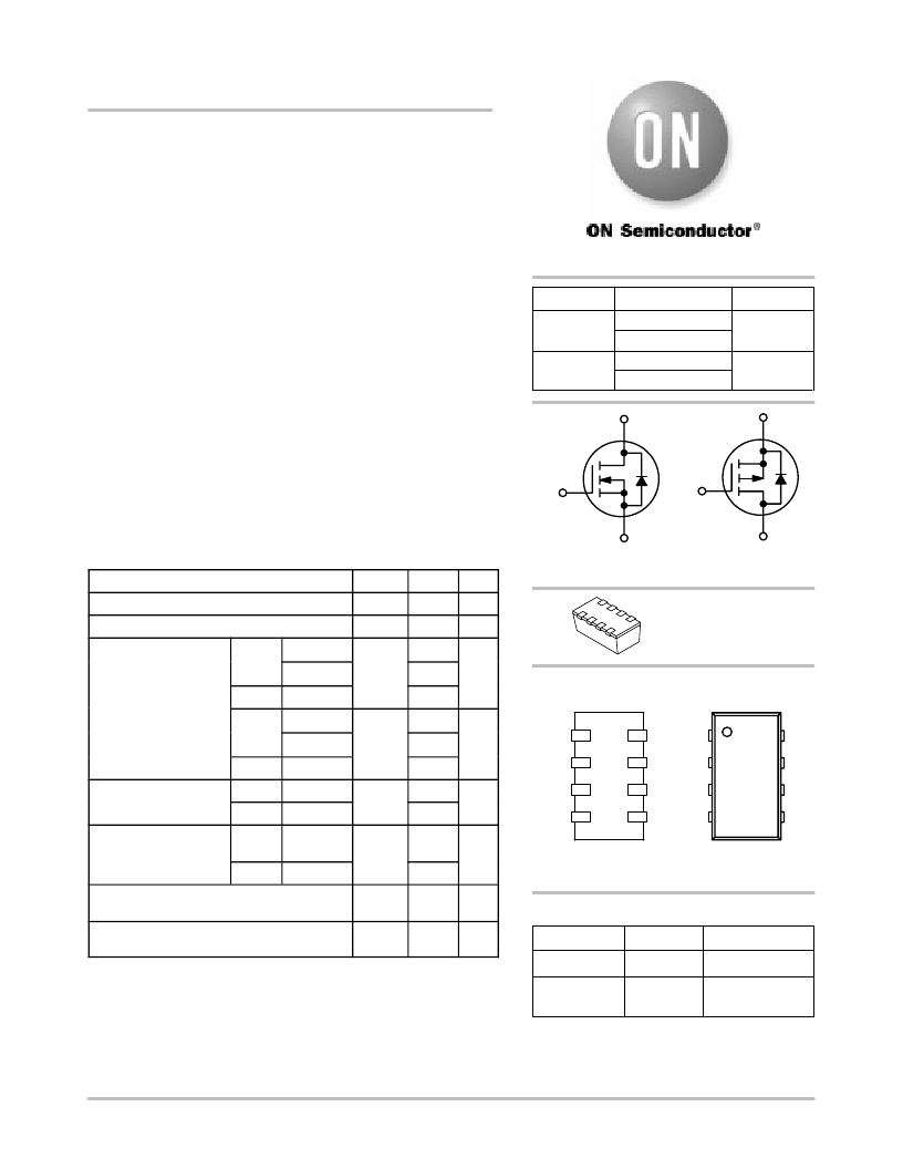
�D� 1�
�G� 1� G� 2�
�I� D� MAX�
�3.9� A�
�?3.0� A�
�S2�
�Powered� Products�
�MAXIMUM� RATINGS� (T� J� =� 25� °� C� unless� otherwise� noted)�
�S� 1�
�N?Channel� MOSFET�
�D� 2�
�P?Channel� MOSFET�
�Parameter�
�Symbol�
�Value�
�Unit�
�Drain?to?Source� Voltage�
�Gate?to?Source� Voltage�
�V� DSS�
�V� GS�
�20�
�±� 12�
�V�
�V�
�ChipFET�
�CASE� 1206A�
�Continuous� Drain�
�Current� (Note� 1)�
�N?Ch�
�Steady�
�State�
�T� A� =� 25� °� C�
�T� A� =� 85� °� C�
�I� D�
�2.9�
�2.1�
�A�
�PIN�
�STYLE� 2�
�MARKING�
�t� v� 5�
�T� A� =� 25� °� C�
�3.9�
�CONNECTIONS�
�DIAGRAM�
�P?Ch�
�Steady�
�State�
�t� v� 5�
�T� A� =� 25� °� C�
�T� A� =� 85� °� C�
�T� A� =� 25� °� C�
�I� D�
�?2.2�
�?1.6�
�?3.0�
�A�
�D� 1�
�D� 1�
�8�
�7�
�1�
�2�
�S� 1�
�G� 1�
�1�
�2�
�8�
�7�
�Pulsed� Drain� Current�
�(Note� 1)�
�N?Ch�
�P?Ch�
�t� =� 10� m� s�
�t� =� 10� m� s�
�I� DM�
�12�
�?9.0�
�A�
�D� 2�
�D� 2�
�6�
�5�
�3�
�4�
�S� 2�
�G� 2�
�3�
�4�
�6�
�5�
�Power� Dissipation�
�(Note� 1)�
�Steady�
�State�
�T� A� =� 25� °� C�
�P� D�
�1.1�
�W�
�t� v� 5�
�Operating� Junction� and� Storage�
�Temperature�
�T� A� =� 25� °� C�
�T� J� ,�
�T� STG�
�2.1�
�?55� to�
�150�
�°� C�
�C1� =� Specific� Device� Code�
�M� =� Month� Code�
�ORDERING� INFORMATION�
�Lead� Temperature� for� Soldering� Purposes�
�(1/8”� from� case� for� 10� seconds)�
�T� L�
�260�
�°� C�
�Device�
�Package�
�Shipping� ?�
�Maximum� ratings� are� those� values� beyond� which� device� damage� can� occur.�
�NTHC5513T1�
�ChipFET�
�3000/Tape� &� Reel�
�Maximum� ratings� applied� to� the� device� are� individual� stress� limit� values� (not�
�normal� operating� conditions)� and� are� not� valid� simultaneously.� If� these� limits� are�
�exceeded,� device� functional� operation� is� not� implied,� damage� may� occur� and�
�NTHC5513T1G�
�ChipFET�
�(Pb?Free)�
�3000/Tape� &� Reel�
�reliability� may� be� affected.�
�1.� Surface� Mounted� on� FR4� board� using� 1� in� sq� pad� size� (Cu� area� =� 1.127� in� sq�
�[1� oz]� including� traces).�
�?For� information� on� tape� and� reel� specifications,�
�including� part� orientation� and� tape� sizes,� please�
�refer� to� our� Tape� and� Reel� Packaging� Specifications�
�Brochure,� BRD8011/D.�
�?� Semiconductor� Components� Industries,� LLC,� 2004�
�October,� 2004� ?� Rev.� 4�
�1�
�Publication� Order� Number:�
�NTHC5513/D�
�相关PDF资料 |
PDF描述 |
|---|---|
| 34BWSP12B4M2RT | TOG MINI S SPDT O-N-O N PC LF |
| 34BWSP31B4M2RT | TOG MINI S SPDT O-O-O N PC LF |
| B12JV | SWITCH TOGGLE SPDT .4VA VRT BRKT |
| B32621A682K | FILM CAP 0.0068UF 10% 1KV |
| B32621A5104K | FILM CAP 0.1000UF 10% 160V |
相关代理商/技术参数 |
参数描述 |
|---|---|
| NTHC5513T1G | 制造商:ON Semiconductor 功能描述:DUAL N/P CHANNEL MOSFET 20V 1206A |
| NTHC60A3 | 制造商:未知厂家 制造商全称:未知厂家 功能描述:Crystal Clock Oscillator |
| NTHC60AA3 | 制造商:未知厂家 制造商全称:未知厂家 功能描述:Crystal Clock Oscillator |
| NTHC60B3 | 制造商:未知厂家 制造商全称:未知厂家 功能描述:Crystal Clock Oscillator |
| NTHC60C3 | 制造商:未知厂家 制造商全称:未知厂家 功能描述:Crystal Clock Oscillator |
发布紧急采购,3分钟左右您将得到回复。