- 您现在的位置:买卖IC网 > PDF目录18311 > NTHD4502NT1G (ON Semiconductor)MOSFET 2N-CH 30V 2.9A CHIPFET PDF资料下载
参数资料
| 型号: | NTHD4502NT1G |
| 厂商: | ON Semiconductor |
| 文件页数: | 2/6页 |
| 文件大小: | 0K |
| 描述: | MOSFET 2N-CH 30V 2.9A CHIPFET |
| 产品目录绘图: | MOSFET ChipFET |
| 标准包装: | 10 |
| FET 型: | 2 个 N 沟道(双) |
| FET 特点: | 逻辑电平门 |
| 漏极至源极电压(Vdss): | 30V |
| 电流 - 连续漏极(Id) @ 25° C: | 2.2A |
| 开态Rds(最大)@ Id, Vgs @ 25° C: | 85 毫欧 @ 2.9A,10V |
| Id 时的 Vgs(th)(最大): | 3V @ 250µA |
| 闸电荷(Qg) @ Vgs: | 7nC @ 10V |
| 输入电容 (Ciss) @ Vds: | 140pF @ 15V |
| 功率 - 最大: | 640mW |
| 安装类型: | 表面贴装 |
| 封装/外壳: | 8-SMD,扁平引线 |
| 供应商设备封装: | ChipFET? |
| 包装: | 标准包装 |
| 产品目录页面: | 1558 (CN2011-ZH PDF) |
| 其它名称: | NTHD4502NT1GOSDKR |
�� �
�
�NTHD4502N�
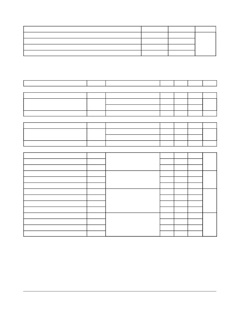
�THERMAL� RESISTANCE� RATINGS�
�Parameter�
�Junction� ?� to� ?� Ambient� –� Steady� State� (Note� 4)�
�Junction� ?� to� ?� Ambient� –� t� ≤� 5� s� (Note� 4)�
�Junction� ?� to� ?� Ambient� –� Steady� State� (Note� 5)�
�Junction� ?� to� ?� Foot� –� Steady� State� (Note� 5)�
�Symbol�
�R� q� JA�
�R� q� JA�
�R� q� JA�
�R� q� JF�
�Max�
�110�
�60�
�195�
�40�
�Unit�
�°� C/W�
�4.� Surface� Mounted� on� FR4� Board� using� 1� in� sq� pad� size� (Cu� area� =� 1.127� in� sq� [1� oz]� including� traces).�
�5.� Surface� Mounted� on� FR4� Board� using� the� minimum� recommended� pad� size� (Cu� area� =� 0.214� in� sq).�
�ELECTRICAL� CHARACTERISTICS� (T� J� =� 25� °� C� unless� otherwise� noted)�
�Parameter�
�Symbol�
�Test� Conditions�
�Min�
�Typ�
�Max�
�Units�
�OFF� CHARACTERISTICS�
�Drain� ?� to� ?� Source� Breakdown� Voltage�
�Zero� Gate� Voltage� Drain� Current�
�V� (BR)DSS�
�I� DSS�
�V� GS� =� 0� V,� I� D� =� 250� m� A�
�V� GS� =� 0� V,� V� DS� =� 24� V�
�30�
�36�
�1.0�
�V�
�m� A�
�V� GS� =� 0� V,� V� DS� =� 24� V,� T� J� =� 125� °� C�
�10�
�Gate� ?� to� ?� Source� Leakage� Current�
�I� GSS�
�V� DS� =� 0� V,� V� GS� =� "� 20� V�
�"� 100�
�nA�
�ON� CHARACTERISTICS� (Note� 6)�
�Gate� Threshold� Voltage�
�Drain� ?� to� ?� Source� On� ?� Resistance�
�V� GS(TH)�
�R� DS(on)�
�V� GS� =� V� DS� ,� I� D� =� 250� m� A�
�V� GS� =� 10� V,� I� D� =� 2.9� A�
�1.0�
�1.65�
�78�
�3.0�
�85�
�V�
�m� W�
�V� GS� =� 4.5� V,� I� D� =� 2.2� A�
�105�
�140�
�Forward� Transconductance�
�g� FS�
�V� DS� =� 15� V,� I� D� =� 2.9� A�
�3.8�
�S�
�CHARGES� AND� CAPACITANCES�
�Input� Capacitance�
�C� ISS�
�140�
�pF�
�Output� Capacitance�
�Reverse� Transfer� Capacitance�
�C� OSS�
�C� RSS�
�V� GS� =� 0� V,� f� =� 1.0� MHz,�
�V� DS� =� 15� V�
�53�
�16�
�Input� Capacitance�
�C� ISS�
�135�
�250�
�pF�
�Output� Capacitance�
�Reverse� Transfer� Capacitance�
�C� OSS�
�C� RSS�
�V� GS� =� 0� V,� f� =� 1.0� MHz,�
�V� DS� =� 24� V�
�42�
�13�
�75�
�25�
�Total� Gate� Charge�
�Threshold� Gate� Charge�
�Gate� ?� to� ?� Source� Charge�
�Gate� ?� to� ?� Drain� Charge�
�Total� Gate� Charge�
�Threshold� Gate� Charge�
�Gate� ?� to� ?� Source� Charge�
�Gate� ?� to� ?� Drain� Charge�
�Q� G(TOT)�
�Q� G(TH)�
�Q� GS�
�Q� GD�
�Q� G(TOT)�
�Q� G(TH)�
�Q� GS�
�Q� GD�
�V� GS� =� 10� V,� V� DS� =� 15� V,�
�I� D� =� 2.9� A�
�V� GS� =� 4.5� V,� V� DS� =� 24� V,�
�I� D� =� 2.9� A�
�3.6�
�0.3�
�0.6�
�0.7�
�1.9�
�0.3�
�0.6�
�0.9�
�7.0�
�nC�
�nC�
�6.� Pulse� Test:� Pulse� Width� v� 300� m� s,� Duty� Cycle� v� 2%.�
�http://onsemi.com�
�2�
�相关PDF资料 |
PDF描述 |
|---|---|
| B32652A1722J | FILM CAP 7.2NF 5% 1600V MKP |
| B32621A4223K | FILM CAP 0.0220UF 10% 400V |
| B32621A392K | FILM CAP 0.0039UF 10% 1KV |
| B32620J332J | FILM CAP 0.0033UF 5% 1KV |
| 34ASP18T7V3RT | TOG MINI SPDT O-N-O T VB LF |
相关代理商/技术参数 |
参数描述 |
|---|---|
| NTHD4508N | 制造商:ONSEMI 制造商全称:ON Semiconductor 功能描述:Power MOSFET 20 V, 4.1 A, Dual N−Channel ChipFET |
| NTHD4508NT1 | 功能描述:MOSFET 20V 4.1A Dual RoHS:否 制造商:STMicroelectronics 晶体管极性:N-Channel 汲极/源极击穿电压:650 V 闸/源击穿电压:25 V 漏极连续电流:130 A 电阻汲极/源极 RDS(导通):0.014 Ohms 配置:Single 最大工作温度: 安装风格:Through Hole 封装 / 箱体:Max247 封装:Tube |
| NTHD4508NT1G | 功能描述:MOSFET 20V 4.1A Dual N-Channel RoHS:否 制造商:STMicroelectronics 晶体管极性:N-Channel 汲极/源极击穿电压:650 V 闸/源击穿电压:25 V 漏极连续电流:130 A 电阻汲极/源极 RDS(导通):0.014 Ohms 配置:Single 最大工作温度: 安装风格:Through Hole 封装 / 箱体:Max247 封装:Tube |
| NTHD4N02 | 制造商:ONSEMI 制造商全称:ON Semiconductor 功能描述:Typical Uses for FETKY Devices |
| NTHD4N02F | 制造商:ONSEMI 制造商全称:ON Semiconductor 功能描述:Power MOSFET and Schottky Diode |
发布紧急采购,3分钟左右您将得到回复。