- 您现在的位置:买卖IC网 > Datasheet目录493 > NTTFS4824NTWG (ON Semiconductor)MOSFET N-CH 30V 8.3A 8WDFN Datasheet资料下载
参数资料
| 型号: | NTTFS4824NTWG |
| 厂商: | ON Semiconductor |
| 文件页数: | 1/6页 |
| 文件大小: | 0K |
| 描述: | MOSFET N-CH 30V 8.3A 8WDFN |
| 产品变化通告: | Product Obsolescence 14/Apr/2010 |
| 标准包装: | 5,000 |
| FET 型: | MOSFET N 通道,金属氧化物 |
| FET 特点: | 逻辑电平门 |
| 漏极至源极电压(Vdss): | 30V |
| 电流 - 连续漏极(Id) @ 25° C: | 8.3A |
| 开态Rds(最大)@ Id, Vgs @ 25° C: | 5 毫欧 @ 20A,10V |
| Id 时的 Vgs(th)(最大): | 2.5V @ 250µA |
| 闸电荷(Qg) @ Vgs: | 18nC @ 4.5V |
| 输入电容 (Ciss) @ Vds: | 2363pF @ 12V |
| 功率 - 最大: | 660mW |
| 安装类型: | 表面贴装 |
| 封装/外壳: | 8-WDFN 裸露焊盘 |
| 供应商设备封装: | 8-WDFN(3.3x3.3) |
| 包装: | 带卷 (TR) |
�� �
�
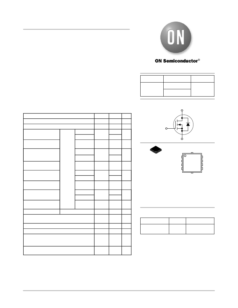
�NTTFS4824N�
�Power� MOSFET�
�30� V,� 69� A,� Single� N� ?� Channel,� m� 8FL�
�Features�
�?� Small� Footprint� (3.3� x� 3.3� mm)� for� Compact� Design�
�?� Low� R� DS(on)� to� Minimize� Conduction� Losses�
�?� Low� Capacitance� to� Minimize� Driver� Losses�
�?� These� Devices� are� Pb� ?� Free,� Halogen� Free/BFR� Free� and� are� RoHS�
�Compliant�
�Applications�
�?� DC� ?� DC� Converters�
�?� Low� Side� Switching�
�MAXIMUM� RATINGS� (T� J� =� 25� °� C� unless� otherwise� stated)�
�V� (BR)DSS�
�30� V�
�http://onsemi.com�
�R� DS(on)� MAX�
�5.0� m� W� @� 10� V�
�7.5� m� W� @� 4.5� V�
�N� ?� Channel� MOSFET�
�D� (5� ?� 8)�
�I� D� MAX�
�69� A�
�Parameter�
�Drain� ?� to� ?� Source� Voltage�
�Symbol�
�V� DSS�
�Value�
�30�
�Unit�
�V�
�Gate� ?� to� ?� Source� Voltage�
�Continuous� Drain�
�Current� R� q� JA� (Note� 1)�
�Power� Dissipation� R� q� JA�
�(Note� 1)�
�Continuous� Drain�
�Current� R� q� JA� ≤� 10� s�
�(Note� 1)�
�Power� Dissipation�
�R� q� JA� ≤� 10� s� (Note� 1)�
�Continuous� Drain�
�Current� R� q� JA� (Note� 2)�
�Steady�
�State�
�T� A� =� 25� °� C�
�T� A� =� 85� °� C�
�T� A� =� 25� °� C�
�T� A� =� 25� °� C�
�T� A� =� 85� °� C�
�T� A� =� 25� °� C�
�T� C� =� 25� °� C�
�T� C� =� 85� °� C�
�V� GS�
�I� D�
�P� D�
�I� D�
�P� D�
�I� D�
�±� 20�
�14.9�
�10.8�
�2.2�
�20.6�
�14.9�
�4.1�
�8.3�
�6.0�
�V�
�A�
�W�
�A�
�W�
�A�
�G� (4)�
�1�
�WDFN8�
�(� m� 8FL)�
�CASE� 511AB�
�FLAT� LEAD�
�4824�
�S� (1,2,3)�
�MARKING� DIAGRAM�
�1�
�S� D�
�S� 4824� D�
�S� AYWW� G� D�
�G� G� D�
�=� Specific� Device� Code�
�Power� Dissipation�
�R� q� JA� (Note� 2)�
�Continuous� Drain�
�Current� R� q� JC� (Note� 1)�
�Power� Dissipation�
�R� q� JC� (Note� 1)�
�T� C� =� 25� °� C�
�T� C� =� 25� °� C�
�T� C� =� 85� °� C�
�T� C� =� 25� °� C�
�P� D�
�I� D�
�P� D�
�0.66�
�69�
�50�
�46.3�
�W�
�A�
�W�
�A� =� Assembly� Location�
�Y� =� Year�
�WW� =� Work� Week�
�G� =� Pb� ?� Free� Package�
�(Note:� Microdot� may� be� in� either� location)�
�Pulsed� Drain� Current� T� A� =� 25� °� C,� t� p� =� 10� m� s�
�Operating� Junction� and� Storage� Temperature�
�I� DM�
�T� J� ,�
�T� stg�
�207�
�?� 55� to�
�+150�
�A�
�°� C�
�ORDERING� INFORMATION�
�Device� Package� Shipping� ?�
�Source� Current� (Body� Diode)�
�I� S�
�46.3�
�A�
�NTTFS4824NTAG�
�WDFN8�
�1500/Tape� &� Reel�
�Drain� to� Source� dV/dt�
�Single� Pulse� Drain� ?� to� ?� Source� Avalanche� Energy�
�(T� J� =� 25� °� C,� V� DD� =� 50� V,� V� GS� =� 10� V,�
�I� L� =� 38� A� pk� ,� L� =� 0.1� mH,� R� G� =� 25� W� )�
�Lead� Temperature� for� Soldering� Purposes�
�(1/8� ″� from� case� for� 10� s)�
�dV/dt�
�E� AS�
�T� L�
�6.0�
�72�
�260�
�V/ns�
�mJ�
�°� C�
�(Pb� ?� Free)�
�?For� information� on� tape� and� reel� specifications,�
�including� part� orientation� and� tape� sizes,� please�
�refer� to� our� Tape� and� Reel� Packaging� Specification�
�Brochure,� BRD8011/D.�
�Stresses� exceeding� Maximum� Ratings� may� damage� the� device.� Maximum�
�Ratings� are� stress� ratings� only.� Functional� operation� above� the� Recommended�
�Operating� Conditions� is� not� implied.� Extended� exposure� to� stresses� above� the�
�Recommended� Operating� Conditions� may� affect� device� reliability.�
�1.� Surface� ?� mounted� on� FR4� board� using� 1� sq� ?� in� pad,� 1� oz� Cu.�
�2.� Surface� ?� mounted� on� FR4� board� using� the� minimum� recommended� pad� size.�
�?� Semiconductor� Components� Industries,� LLC,� 2013�
�September,� 2013� ?� Rev.� 5�
�1�
�Publication� Order� Number:�
�NTTFS4824N/D�
�相关PDF资料 |
PDF描述 |
|---|---|
| NTTFS4840NTAG | MOSFET N-CH 30V 4.6A 8WDFN |
| NTTFS4928NTAG | MOSFET N-CH 30V 7.3A 8WDFN |
| NTTFS4929NTAG | MOSFET N-CH 30V 34A 8WDFN |
| NTTFS4930NTWG | MOSFET N-CH 30V 23A 8WDFN |
| NTTFS4932NTAG | MOSFET N-CH 30V 11A 8WDFN |
相关代理商/技术参数 |
参数描述 |
|---|---|
| NTTFS4840N | 制造商:ONSEMI 制造商全称:ON Semiconductor 功能描述:Power MOSFET 30 V, 26 A, Single N−Channel, μ8FL |
| NTTFS4840NTAG | 功能描述:MOSFET NFET U8FL 30V 26A 24MO RoHS:否 制造商:STMicroelectronics 晶体管极性:N-Channel 汲极/源极击穿电压:650 V 闸/源击穿电压:25 V 漏极连续电流:130 A 电阻汲极/源极 RDS(导通):0.014 Ohms 配置:Single 最大工作温度: 安装风格:Through Hole 封装 / 箱体:Max247 封装:Tube |
| NTTFS4840NTWG | 功能描述:MOSFET NFET U8FL 30V 26A 24mOHM RoHS:否 制造商:STMicroelectronics 晶体管极性:N-Channel 汲极/源极击穿电压:650 V 闸/源击穿电压:25 V 漏极连续电流:130 A 电阻汲极/源极 RDS(导通):0.014 Ohms 配置:Single 最大工作温度: 安装风格:Through Hole 封装 / 箱体:Max247 封装:Tube |
| NTTFS4928N | 制造商:ONSEMI 制造商全称:ON Semiconductor 功能描述:Power MOSFET 30 V, 37 A, Single N?Channel, 8FL DC?DC Converters |
| NTTFS4928NTAG | 功能描述:MOSFET NFET U8FL 30V 41A 8MOHM RoHS:否 制造商:STMicroelectronics 晶体管极性:N-Channel 汲极/源极击穿电压:650 V 闸/源击穿电压:25 V 漏极连续电流:130 A 电阻汲极/源极 RDS(导通):0.014 Ohms 配置:Single 最大工作温度: 安装风格:Through Hole 封装 / 箱体:Max247 封装:Tube |
发布紧急采购,3分钟左右您将得到回复。