- 您现在的位置:买卖IC网 > PDF目录6028 > OP484FSZ-REEL7 (Analog Devices Inc)IC OPAMP GP R-R 4.25MHZ 14SOIC PDF资料下载
参数资料
| 型号: | OP484FSZ-REEL7 |
| 厂商: | Analog Devices Inc |
| 文件页数: | 8/24页 |
| 文件大小: | 0K |
| 描述: | IC OPAMP GP R-R 4.25MHZ 14SOIC |
| 标准包装: | 1 |
| 放大器类型: | 通用 |
| 电路数: | 4 |
| 输出类型: | 满摆幅 |
| 转换速率: | 4 V/µs |
| 增益带宽积: | 4.25MHz |
| 电流 - 输入偏压: | 80nA |
| 电压 - 输入偏移: | 250µV |
| 电流 - 电源: | 2.25mA |
| 电流 - 输出 / 通道: | 10mA |
| 电压 - 电源,单路/双路(±): | 3 V ~ 36 V,±1.5 V ~ 18 V |
| 工作温度: | -40°C ~ 125°C |
| 安装类型: | 表面贴装 |
| 封装/外壳: | 14-SOIC(0.154",3.90mm 宽) |
| 供应商设备封装: | 14-SO |
| 包装: | 剪切带 (CT) |
| 其它名称: | OP484FSZ-REEL7CT |
OP184/OP284/OP484
Rev. J | Page 16 of 24
As a design aid, Figure 49 shows the total equivalent input noise
of the OP284 and the total thermal noise of a resistor for com-
parison. Note that for source resistance less than 1 kΩ, the
equivalent input noise voltage of the OP284 is dominant.
TOTAL SOURCE RESISTANCE, RS ()
100
1
EQ
U
IVA
L
EN
T
H
ER
MA
L
N
O
ISE
(n
V/
H
z)
10
10k
OP284 TOTAL
EQUIVALENT NOISE
RESISTOR THERMAL
NOISE ONLY
00293-
049
100
1k
100k
FREQUENCY = 1kHz
TA = 25°C
Figure 49. OP284 Equivalent Thermal Noise vs. Total Source Resistance
Because circuit SNR is the critical parameter in the final analysis,
the noise behavior of a circuit is often expressed in terms of its
noise figure, NF. The noise figure is defined as the ratio of a
circuit’s output signal-to-noise to its input signal-to-noise.
An expression of a circuit NF in dB, and in terms of the
operational amplifier voltage and current noise parameters
defined previously, is given by
( )
(
)
( )
×
+
=
2
1
log
10
dB
nRS
S
nOA
e
R
i
e
NF
where:
NF (dB) is the noise figure of the circuit, expressed in decibels.
(enOA)2 is the OP284 noise voltage spectral power (1 Hz bandwidth).
(inOA)2 is the OP284 noise current spectral power (1 Hz bandwidth).
(enRS)2 is the source resistance thermal noise voltage power =
(4kTRS).
RS is the effective, or equivalent, source resistance presented to
the amplifier.
Calculation of the circuit noise figure is straightforward because
the signal level in the application is not required to determine it.
However, many designers using NF calculations as the basis for
achieving optimum SNR believe that a low noise figure is equal to
low total noise. In fact, the opposite is true, as shown in Figure 50.
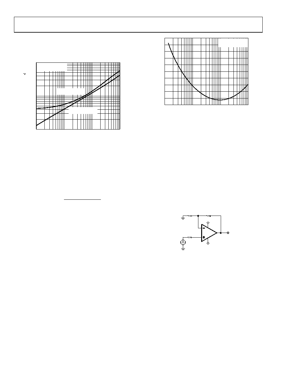
The noise figure of the OP284 is expressed as a function of
the source resistance level. Note that the lowest noise figure for
the OP284 occurs at a source resistance level of 10 kΩ.
However, Figure 49 shows that this source resistance level and
the OP284 generate approximately 14 nV/√Hz of total
equivalent circuit noise. Signal levels in the application
invariably increase to maximize circuit SNR, which is not an
option in low voltage, single-supply applications.
TOTAL SOURCE RESISTANCE, RS ()
10
100
N
OIS
E
FIGU
R
E
(
dB
)
5
10k
100k
1k
0
9
8
7
6
4
3
2
1
00293-
050
FREQUENCY = 1kHz
TA = 25°C
Figure 50. OP284 Noise Figure vs. Source Resistance
Therefore, to achieve optimum circuit SNR in single-supply
applications, it is recommended that an operational amplifier
with the lowest equivalent input noise voltage be chosen, along
with source resistance levels that are consistent with maintaining
low total circuit noise.
OVERDRIVE RECOVERY
The overdrive recovery time of an operational amplifier is the
time required for the output voltage to recover to its linear region
from a saturated condition. The recovery time is important in
applications where the amplifier must recover quickly after a
large transient event. The circuit shown in Figure 51 was used
to evaluate the OP284 overload recovery time. The OP284
takes approximately 2 s to recover from positive saturation
and approximately 1 s to recover from negative saturation.
2
3
1
+5V
8
4
R1
10k
R3
9k
R2
10k
VIN
10V STEP
–5V
VOUT
1/2
OP284
00293-
051
Figure 51. Output Overload Recovery Test Circuit
SINGLE-SUPPLY, 3 V INSTRUMENTATION
AMPLIFIER
The low noise, wide bandwidth, and rail-to-rail input/output
operation of the OP284 make it ideal for low supply voltage
applications such as in the two op amp instrumentation amplifier
shown in Figure 52. The circuit uses the classic two op amp
instrumentation amplifier topology with four resistors to set the
gain. The transfer equation of the circuit is identical to that of a
noninverting amplifier. Resistor R2 and Resistor R3 should be
closely matched to each other, as well as to Resistors (R1 + P1)
and Resistor R4 to ensure good common-mode rejection
performance.
相关PDF资料 |
PDF描述 |
|---|---|
| AD8221BRZ | IC AMP INSTRUMENT PREC HP 8SOIC |
| OP293ESZ | IC OPAMP GP 35KHZ DUAL 8SOIC |
| PBC12SFDN | CONN HEADER .100 SINGL STR 12POS |
| AD8250ARMZ | IC AMP INST ICMOS LDRIFT 10MSOP |
| 929836-05-01-RK | CONN HEADER .100 DUAL STR 2POS |
相关代理商/技术参数 |
参数描述 |
|---|---|
| OP490 | 制造商:AD 制造商全称:Analog Devices 功能描述:Low Voltage Micropower Quad Operational Amplifier |
| OP4900046S | 制造商:Rochester Electronics LLC 功能描述:- Bulk |
| OP490019S | 制造商:Analog Devices 功能描述: |
| OP490-019S | 制造商:Analog Devices 功能描述: |
| OP490ATC/883 | 制造商:AD 制造商全称:Analog Devices 功能描述:Low Voltage Micropower Quad Operational Amplifier |
发布紧急采购,3分钟左右您将得到回复。