- 您现在的位置:买卖IC网 > PDF目录189414 > OR2T10A-4S256 (Electronic Theatre Controls, Inc.) Field-Programmable Gate Arrays PDF资料下载
参数资料
| 型号: | OR2T10A-4S256 |
| 厂商: | Electronic Theatre Controls, Inc. |
| 元件分类: | FPGA |
| 英文描述: | Field-Programmable Gate Arrays |
| 中文描述: | 现场可编程门阵列 |
| 文件页数: | 145/192页 |
| 文件大小: | 3148K |
| 代理商: | OR2T10A-4S256 |
第1页第2页第3页第4页第5页第6页第7页第8页第9页第10页第11页第12页第13页第14页第15页第16页第17页第18页第19页第20页第21页第22页第23页第24页第25页第26页第27页第28页第29页第30页第31页第32页第33页第34页第35页第36页第37页第38页第39页第40页第41页第42页第43页第44页第45页第46页第47页第48页第49页第50页第51页第52页第53页第54页第55页第56页第57页第58页第59页第60页第61页第62页第63页第64页第65页第66页第67页第68页第69页第70页第71页第72页第73页第74页第75页第76页第77页第78页第79页第80页第81页第82页第83页第84页第85页第86页第87页第88页第89页第90页第91页第92页第93页第94页第95页第96页第97页第98页第99页第100页第101页第102页第103页第104页第105页第106页第107页第108页第109页第110页第111页第112页第113页第114页第115页第116页第117页第118页第119页第120页第121页第122页第123页第124页第125页第126页第127页第128页第129页第130页第131页第132页第133页第134页第135页第136页第137页第138页第139页第140页第141页第142页第143页第144页当前第145页第146页第147页第148页第149页第150页第151页第152页第153页第154页第155页第156页第157页第158页第159页第160页第161页第162页第163页第164页第165页第166页第167页第168页第169页第170页第171页第172页第173页第174页第175页第176页第177页第178页第179页第180页第181页第182页第183页第184页第185页第186页第187页第188页第189页第190页第191页第192页
Data Sheet
ORCA Series 2 FPGAs
June 1999
56
Lucent Technologies Inc.
Special Function Blocks (continued)
There are four
ORCA-defined instructions. The PLC
scan rings 1 and 2 (PSR1, PSR2) allow user-defined
internal scan paths using the PLC latches/FFs. The
RAM_Write Enable (RAM_W) instruction allows the
user to serially configure the FPGA through TDI. The
RAM_Read Enable (RAM_R) allows the user to read
back RAM contents on TDO after configuration.
ORCA Boundary-Scan Circuitry
The
ORCA Series boundary-scan circuitry includes a
test access port controller (TAPC), instruction register
(IR), boundary-scan register (BSR), and bypass regis-
ter. It also includes circuitry to support the four pre-
defined instructions.
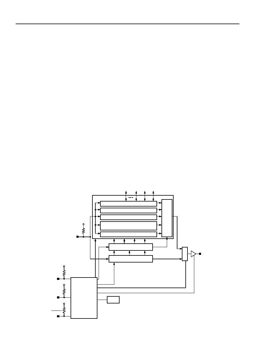
Figure 49 shows a functional diagram of the boundary-
scan circuitry that is implemented in the
ORCA series.
The input pins’ (TMS, TCK, and TDI) locations vary
depending on the part, and the output pin is the dedi-
cated TDO/RD_DATA output pad. Test data in (TDI) is
the serial input data. Test mode select (TMS) controls
the boundary-scan test access port controller (TAPC).
Test clock (TCK) is the test clock on the board.
The BSR is a series connection of boundary-scan cells
(BSCs) around the periphery of the IC. Each I/O pad on
the FPGA, except for CCLK, DONE, and the boundary-
scan pins (TCK, TDI, TMS, and TDO), is included in
the BSR. The first BSC in the BSR (connected to TDI)
is located in the first PIC I/O pad on the left of the top
side of the FPGA (PTA PIC). The BSR proceeds clock-
wise around the top, right, bottom, and left sides of the
array. The last BSC in the BSR (connected to TDO) is
located on the top of the left side of the array (PLA3).
The bypass instruction uses a single FF which resyn-
chronizes test data that is not part of the current scan
operation. In a bypass instruction, test data received on
TDI is shifted out of the bypass register to TDO. Since
the BSR (which requires a two FF delay for each pad)
is bypassed, test throughput is increased when devices
that are not part of a test operation are bypassed.
The boundary-scan logic is enabled before and during
configuration. After configuration, a configuration
option determines whether or not boundary-scan logic
is used.
The 32-bit boundary-scan identification register con-
tains the manufacturer’s ID number, unique part num-
ber, and version, but is not implemented in the
ORCA
series of FPGAs. If boundary scan is not used, TMS,
TDI, and TCK become user I/Os, and TDO is 3-stated
or used in the readback operation.
5-2840(C).r7
Figure 49.
ORCA Series Boundary-Scan Circuitry Functional Diagram
TAP
CONTROLLER
BOUNDARY-SCAN REGISTER
PSR2 REGISTER (PLCs)
BYPASS REGISTER
DATA
MUX
INSTRUCTION DECODER
INSTRUCTION REGISTER
M
U
X
RESET
CLOCK-IR
SHIFT-IR
UPDATE-IR
PUR
TDO
SELECT
ENABLE
RESET
CLOCK-DR
SHIFT-DR
UPDATE-DR
TDI
DATA REGISTERS
PSR1 REGISTER (PLCs)
CONFIGURATION REGISTER
(RAM_R, RAM_W)
I/O BUFFERS
VDD
TMS
VDD
TCK
VDD
PRGM
VDD
相关PDF资料 |
PDF描述 |
|---|---|
| OR2T10A-4S240I | Field-Programmable Gate Arrays |
| OR2T10A-4S240 | Field-Programmable Gate Arrays |
| OR2T10A-4S208I | Field-Programmable Gate Arrays |
| OR2T10A-4S208 | Ceramic Chip Capacitors / MIL-PRF-55681; Capacitance [nom]: 47pF; Working Voltage (Vdc)[max]: 100V; Capacitance Tolerance: +/-5%; Dielectric: Multilayer Ceramic; Temperature Coefficient: C0G (NP0); Lead Style: Surface Mount Chip; Lead Dimensions: 1206; Termination: Solder Coated SnPb; Body Dimensions: 0.125" x 0.062" x 0.051"; Container: Bag; Features: MIL-PRF-55681: R Failure Rate |
| OR2T10A-4S160I | Field-Programmable Gate Arrays |
相关代理商/技术参数 |
参数描述 |
|---|---|
| OR2T10A5BA256-DB | 功能描述:FPGA - 现场可编程门阵列 1024 LUT 244 I/O RoHS:否 制造商:Altera Corporation 系列:Cyclone V E 栅极数量: 逻辑块数量:943 内嵌式块RAM - EBR:1956 kbit 输入/输出端数量:128 最大工作频率:800 MHz 工作电源电压:1.1 V 最大工作温度:+ 70 C 安装风格:SMD/SMT 封装 / 箱体:FBGA-256 |
| OR2T10A5J160-DB | 功能描述:FPGA - 现场可编程门阵列 1024 LUT 244 I/O RoHS:否 制造商:Altera Corporation 系列:Cyclone V E 栅极数量: 逻辑块数量:943 内嵌式块RAM - EBR:1956 kbit 输入/输出端数量:128 最大工作频率:800 MHz 工作电源电压:1.1 V 最大工作温度:+ 70 C 安装风格:SMD/SMT 封装 / 箱体:FBGA-256 |
| OR2T10A5S208-DB | 功能描述:FPGA - 现场可编程门阵列 1024 LUT 244 I/O RoHS:否 制造商:Altera Corporation 系列:Cyclone V E 栅极数量: 逻辑块数量:943 内嵌式块RAM - EBR:1956 kbit 输入/输出端数量:128 最大工作频率:800 MHz 工作电源电压:1.1 V 最大工作温度:+ 70 C 安装风格:SMD/SMT 封装 / 箱体:FBGA-256 |
| OR2T10A5S240-DB | 功能描述:FPGA - 现场可编程门阵列 Use ECP/EC or XP RoHS:否 制造商:Altera Corporation 系列:Cyclone V E 栅极数量: 逻辑块数量:943 内嵌式块RAM - EBR:1956 kbit 输入/输出端数量:128 最大工作频率:800 MHz 工作电源电压:1.1 V 最大工作温度:+ 70 C 安装风格:SMD/SMT 封装 / 箱体:FBGA-256 |
| OR2T12A4BA256-DB | 制造商:Rochester Electronics LLC 功能描述:- Bulk 制造商:Lattice Semiconductor Corporation 功能描述: |
发布紧急采购,3分钟左右您将得到回复。