- 您现在的位置:买卖IC网 > PDF目录189437 > OR2T26A-6S352 (Electronic Theatre Controls, Inc.) Field-Programmable Gate Arrays PDF资料下载
参数资料
| 型号: | OR2T26A-6S352 |
| 厂商: | Electronic Theatre Controls, Inc. |
| 元件分类: | FPGA |
| 英文描述: | Field-Programmable Gate Arrays |
| 中文描述: | 现场可编程门阵列 |
| 文件页数: | 147/192页 |
| 文件大小: | 3148K |
| 代理商: | OR2T26A-6S352 |
第1页第2页第3页第4页第5页第6页第7页第8页第9页第10页第11页第12页第13页第14页第15页第16页第17页第18页第19页第20页第21页第22页第23页第24页第25页第26页第27页第28页第29页第30页第31页第32页第33页第34页第35页第36页第37页第38页第39页第40页第41页第42页第43页第44页第45页第46页第47页第48页第49页第50页第51页第52页第53页第54页第55页第56页第57页第58页第59页第60页第61页第62页第63页第64页第65页第66页第67页第68页第69页第70页第71页第72页第73页第74页第75页第76页第77页第78页第79页第80页第81页第82页第83页第84页第85页第86页第87页第88页第89页第90页第91页第92页第93页第94页第95页第96页第97页第98页第99页第100页第101页第102页第103页第104页第105页第106页第107页第108页第109页第110页第111页第112页第113页第114页第115页第116页第117页第118页第119页第120页第121页第122页第123页第124页第125页第126页第127页第128页第129页第130页第131页第132页第133页第134页第135页第136页第137页第138页第139页第140页第141页第142页第143页第144页第145页第146页当前第147页第148页第149页第150页第151页第152页第153页第154页第155页第156页第157页第158页第159页第160页第161页第162页第163页第164页第165页第166页第167页第168页第169页第170页第171页第172页第173页第174页第175页第176页第177页第178页第179页第180页第181页第182页第183页第184页第185页第186页第187页第188页第189页第190页第191页第192页
Data Sheet
ORCA Series 2 FPGAs
June 1999
58
Lucent Technologies Inc.
Special Function Blocks (continued)
Boundary-Scan Cells
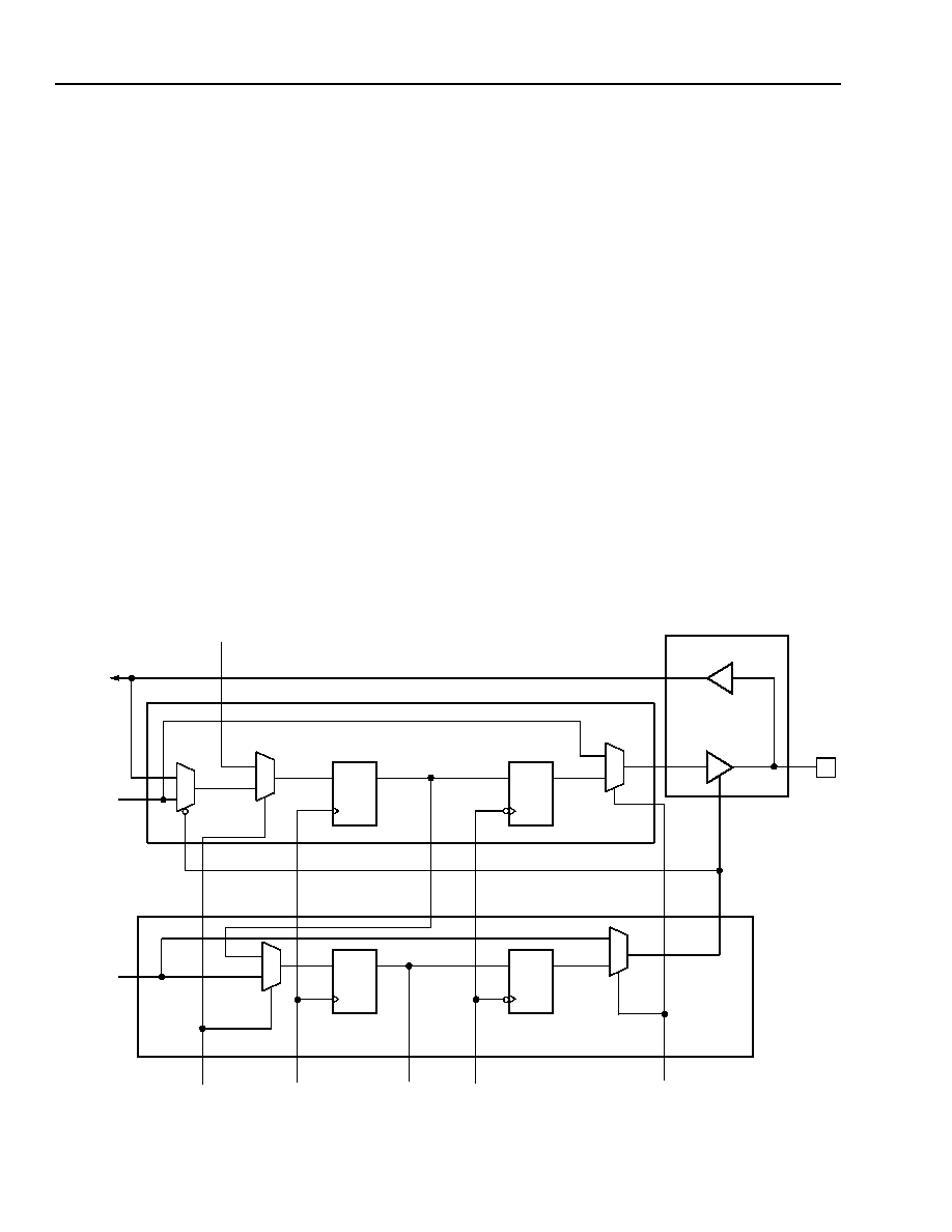
Figure 51 is a diagram of the boundary-scan cell (BSC)
in the
ORCA series PICs. There are four BSCs in each
PIC: one for each pad, except as noted above. The
BSCs are connected serially to form the BSR. The
BSC controls the functionality of the in, out, and 3-state
signals for each pad.
The BSC allows the I/O to function in either the normal
or test mode. Normal mode is defined as when an out-
put buffer receives input from the PLC array and pro-
vides output at the pad or when an input buffer
provides input from the pad to the PLC array. In the test
mode, the BSC executes a boundary-scan operation,
such as shifting in scan data from an upstream BSC in
the BSR, providing test stimuli to the pad, capturing
test data at the pad, etc.
The primary functions of the BSC are shifting scan data
serially in the BSR and observing input (P_IN), output
(P_OUT), and 3-state (P_TS) signals at the pads. The
BSC consists of two circuits: the bidirectional data cell
is used to access the input and output data, and the
direction control cell is used to access the 3-state
value. Both cells consist of a flip-flop used to shift scan
data which feeds a flip-flop to control the I/O buffer. The
bidirectional data cell is connected serially to the direc-
tion control cell to form a boundary-scan shift register.
The TAPC signals (capture, update, shiftn, treset, and
TCK) and the MODE signal control the operation of the
BSC. The bidirectional data cell is also controlled by
the high out/low in (HOLI) signal generated by the
direction control cell. When HOLI is low, the bidirec-
tional data cell receives input buffer data into the BSC.
When HOLI is high, the BSC is loaded with functional
data from the PLC.
The MODE signal is generated from the decode of the
instruction register. When the MODE signal is high
(EXTEST), the scan data is propagated to the output
buffer. When the MODE signal is low (BYPASS or
SAMPLE), functional data from the FPGA’s internal
logic is propagated to the output buffer.
The boundary-scan description language (BSDL) is
provided for each device in the
ORCA series of FPGAs.
The BSDL is generated from a device profile, pinout,
and other boundary-scan information.
5-2844(F).r4
Figure 51. Boundary-Scan Cell
D
Q
D
Q
D
Q
D
Q
SCAN IN
P_OUT
HOLI
BIDIRECTIONAL DATA CELL
I/O BUFFER
DIRECTION CONTROL CELL
MODE
UPDATE/TCK
SCAN OUT
TCK
SHIFTN/CAPTURE
P_TS
P_IN
PAD_IN
PAD_TS
PAD_OUT
0
1
0
1
0
1
0
1
0
1
相关PDF资料 |
PDF描述 |
|---|---|
| OR2T26A-6S352I | Field-Programmable Gate Arrays |
| OR2T26A-6S432 | Field-Programmable Gate Arrays |
| OR2T26A-6S432I | Field-Programmable Gate Arrays |
| OR2T26A-6T208 | Field-Programmable Gate Arrays |
| OR2T26A-6T208I | Field-Programmable Gate Arrays |
相关代理商/技术参数 |
参数描述 |
|---|---|
| OR2T26A7BA352-DB | 功能描述:FPGA - 现场可编程门阵列 2304 LUT 326 I/O RoHS:否 制造商:Altera Corporation 系列:Cyclone V E 栅极数量: 逻辑块数量:943 内嵌式块RAM - EBR:1956 kbit 输入/输出端数量:128 最大工作频率:800 MHz 工作电源电压:1.1 V 最大工作温度:+ 70 C 安装风格:SMD/SMT 封装 / 箱体:FBGA-256 |
| OR2T26A7BC432-DB | 功能描述:FPGA - 现场可编程门阵列 2304 LUT 326 I/O RoHS:否 制造商:Altera Corporation 系列:Cyclone V E 栅极数量: 逻辑块数量:943 内嵌式块RAM - EBR:1956 kbit 输入/输出端数量:128 最大工作频率:800 MHz 工作电源电压:1.1 V 最大工作温度:+ 70 C 安装风格:SMD/SMT 封装 / 箱体:FBGA-256 |
| OR2T26A7PS208-DB | 功能描述:FPGA - 现场可编程门阵列 2304 LUT 326 I/O RoHS:否 制造商:Altera Corporation 系列:Cyclone V E 栅极数量: 逻辑块数量:943 内嵌式块RAM - EBR:1956 kbit 输入/输出端数量:128 最大工作频率:800 MHz 工作电源电压:1.1 V 最大工作温度:+ 70 C 安装风格:SMD/SMT 封装 / 箱体:FBGA-256 |
| OR2T26A7PS240-DB | 功能描述:FPGA - 现场可编程门阵列 2304 LUT 326 I/O RoHS:否 制造商:Altera Corporation 系列:Cyclone V E 栅极数量: 逻辑块数量:943 内嵌式块RAM - EBR:1956 kbit 输入/输出端数量:128 最大工作频率:800 MHz 工作电源电压:1.1 V 最大工作温度:+ 70 C 安装风格:SMD/SMT 封装 / 箱体:FBGA-256 |
| OR2T26A7S208-DB | 功能描述:FPGA - 现场可编程门阵列 Use LatticeEC RoHS:否 制造商:Altera Corporation 系列:Cyclone V E 栅极数量: 逻辑块数量:943 内嵌式块RAM - EBR:1956 kbit 输入/输出端数量:128 最大工作频率:800 MHz 工作电源电压:1.1 V 最大工作温度:+ 70 C 安装风格:SMD/SMT 封装 / 箱体:FBGA-256 |
发布紧急采购,3分钟左右您将得到回复。