- 您现在的位置:买卖IC网 > PDF目录268233 > OR2T40A6BC432I-DB (LATTICE SEMICONDUCTOR CORP) FPGA, 900 CLBS, 43200 GATES, PBGA432 PDF资料下载
参数资料
| 型号: | OR2T40A6BC432I-DB |
| 厂商: | LATTICE SEMICONDUCTOR CORP |
| 元件分类: | FPGA |
| 英文描述: | FPGA, 900 CLBS, 43200 GATES, PBGA432 |
| 封装: | EBGA-432 |
| 文件页数: | 129/196页 |
| 文件大小: | 3475K |
| 代理商: | OR2T40A6BC432I-DB |
第1页第2页第3页第4页第5页第6页第7页第8页第9页第10页第11页第12页第13页第14页第15页第16页第17页第18页第19页第20页第21页第22页第23页第24页第25页第26页第27页第28页第29页第30页第31页第32页第33页第34页第35页第36页第37页第38页第39页第40页第41页第42页第43页第44页第45页第46页第47页第48页第49页第50页第51页第52页第53页第54页第55页第56页第57页第58页第59页第60页第61页第62页第63页第64页第65页第66页第67页第68页第69页第70页第71页第72页第73页第74页第75页第76页第77页第78页第79页第80页第81页第82页第83页第84页第85页第86页第87页第88页第89页第90页第91页第92页第93页第94页第95页第96页第97页第98页第99页第100页第101页第102页第103页第104页第105页第106页第107页第108页第109页第110页第111页第112页第113页第114页第115页第116页第117页第118页第119页第120页第121页第122页第123页第124页第125页第126页第127页第128页当前第129页第130页第131页第132页第133页第134页第135页第136页第137页第138页第139页第140页第141页第142页第143页第144页第145页第146页第147页第148页第149页第150页第151页第152页第153页第154页第155页第156页第157页第158页第159页第160页第161页第162页第163页第164页第165页第166页第167页第168页第169页第170页第171页第172页第173页第174页第175页第176页第177页第178页第179页第180页第181页第182页第183页第184页第185页第186页第187页第188页第189页第190页第191页第192页第193页第194页第195页第196页
Data Sheet
ORCA Series 2 FPGAs
January 2003
38
Lattice Semiconductor
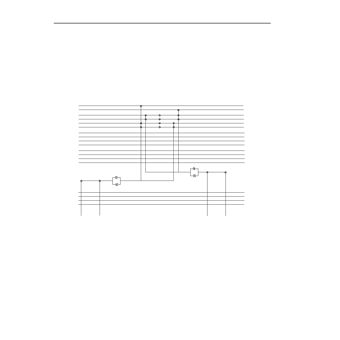
Interquad Routing (continued)
PIC Interquad (MID) Routing
Between the PICs in each quadrant, there is also con-
nectivity between the PIC routing and the interquad
routing. These blocks are called LMID (left), TMID
(top), RMID (right), and BMID (bottom). The TMID rout-
ing is shown in Figure 33. As with the hIQ and vIQ
blocks, the only connectivity to the PIC routing is to the
global PXH and PXL lines.
The PXH lines from the one quadrant can be con-
nected through a CIP to its counterpart in the opposite
quadrant, providing a path that spans the array of PICs.
Since a passive CIP is used to connect the two PXH
lines, a 3-state signal can be routed on the two PXH
lines in the opposite quadrants, and then connected
through this CIP. As with the hIQ and vIQ blocks, CIPs
and buffers allow nibble-wide connections between the
interquad lines, the XH lines, and the XL lines.
5-4201(F).r4
Figure 33. Top (TMID) Routing
PXL[1]
PXL[0]
PX4[3]
PX4[2]
PX4[1]
PX4[0]
PX1[3]
PX1[2]
PX1[1]
PX1[0]
VIQ0[0]
PXH[2]
PXH[1]
PXH[0]
HX4[3]
HX4[2]
HX4[1]
HX4[0]
VIQ1[0]
VIQ2[0]
VIQ3[0]
PXH[3]
PXL[1]
PXL[0]
PX4[3]
PX4[2]
PX4[1]
PX4[0]
PX1[3]
PX1[2]
PX1[1]
PX1[0]
PXH[2]
PXH[1]
PXH[0]
HX4[3]
HX4[2]
HX4[1]
HX4[0]
PXH[3]
相关PDF资料 |
PDF描述 |
|---|---|
| OR2T40A7BC432-DB | FPGA, 900 CLBS, 43200 GATES, PBGA432 |
| OR2C08A-2B256 | FPGA, 196 CLBS, 7000 GATES, PBGA256 |
| OR2C08A-3B256 | FPGA, 196 CLBS, 7000 GATES, PBGA256 |
| OR2C08A-4B256 | FPGA, 196 CLBS, 7000 GATES, PBGA256 |
| OR2C08A-2B256I | FPGA, 196 CLBS, 7000 GATES, PBGA256 |
相关代理商/技术参数 |
参数描述 |
|---|---|
| OR2T40A6PS208-DB | 功能描述:FPGA - 现场可编程门阵列 3600 LUT 326 I/O RoHS:否 制造商:Altera Corporation 系列:Cyclone V E 栅极数量: 逻辑块数量:943 内嵌式块RAM - EBR:1956 kbit 输入/输出端数量:128 最大工作频率:800 MHz 工作电源电压:1.1 V 最大工作温度:+ 70 C 安装风格:SMD/SMT 封装 / 箱体:FBGA-256 |
| OR2T40A6PS208I-DB | 功能描述:FPGA - 现场可编程门阵列 3600 LUT 326 I/O RoHS:否 制造商:Altera Corporation 系列:Cyclone V E 栅极数量: 逻辑块数量:943 内嵌式块RAM - EBR:1956 kbit 输入/输出端数量:128 最大工作频率:800 MHz 工作电源电压:1.1 V 最大工作温度:+ 70 C 安装风格:SMD/SMT 封装 / 箱体:FBGA-256 |
| OR2T40A6PS240DB | 制造商:ORCA 功能描述:NEW |
| OR2T40A6PS240-DB | 功能描述:FPGA - 现场可编程门阵列 3600 LUT 326 I/O RoHS:否 制造商:Altera Corporation 系列:Cyclone V E 栅极数量: 逻辑块数量:943 内嵌式块RAM - EBR:1956 kbit 输入/输出端数量:128 最大工作频率:800 MHz 工作电源电压:1.1 V 最大工作温度:+ 70 C 安装风格:SMD/SMT 封装 / 箱体:FBGA-256 |
| OR2T40A6PS240I-DB | 功能描述:FPGA - 现场可编程门阵列 3600 LUT 326 I/O RoHS:否 制造商:Altera Corporation 系列:Cyclone V E 栅极数量: 逻辑块数量:943 内嵌式块RAM - EBR:1956 kbit 输入/输出端数量:128 最大工作频率:800 MHz 工作电源电压:1.1 V 最大工作温度:+ 70 C 安装风格:SMD/SMT 封装 / 箱体:FBGA-256 |
发布紧急采购,3分钟左右您将得到回复。