- 您现在的位置:买卖IC网 > PDF目录299576 > OR3T55-4PS240 FPGA, 324 CLBS, 40000 GATES, 80 MHz, PQFP240 PDF资料下载
参数资料
| 型号: | OR3T55-4PS240 |
| 元件分类: | FPGA |
| 英文描述: | FPGA, 324 CLBS, 40000 GATES, 80 MHz, PQFP240 |
| 封装: | SQFP-240 |
| 文件页数: | 161/210页 |
| 文件大小: | 2138K |
| 代理商: | OR3T55-4PS240 |
第1页第2页第3页第4页第5页第6页第7页第8页第9页第10页第11页第12页第13页第14页第15页第16页第17页第18页第19页第20页第21页第22页第23页第24页第25页第26页第27页第28页第29页第30页第31页第32页第33页第34页第35页第36页第37页第38页第39页第40页第41页第42页第43页第44页第45页第46页第47页第48页第49页第50页第51页第52页第53页第54页第55页第56页第57页第58页第59页第60页第61页第62页第63页第64页第65页第66页第67页第68页第69页第70页第71页第72页第73页第74页第75页第76页第77页第78页第79页第80页第81页第82页第83页第84页第85页第86页第87页第88页第89页第90页第91页第92页第93页第94页第95页第96页第97页第98页第99页第100页第101页第102页第103页第104页第105页第106页第107页第108页第109页第110页第111页第112页第113页第114页第115页第116页第117页第118页第119页第120页第121页第122页第123页第124页第125页第126页第127页第128页第129页第130页第131页第132页第133页第134页第135页第136页第137页第138页第139页第140页第141页第142页第143页第144页第145页第146页第147页第148页第149页第150页第151页第152页第153页第154页第155页第156页第157页第158页第159页第160页当前第161页第162页第163页第164页第165页第166页第167页第168页第169页第170页第171页第172页第173页第174页第175页第176页第177页第178页第179页第180页第181页第182页第183页第184页第185页第186页第187页第188页第189页第190页第191页第192页第193页第194页第195页第196页第197页第198页第199页第200页第201页第202页第203页第204页第205页第206页第207页第208页第209页第210页
54
Lucent Technologies Inc.
Preliminary Data Sheet, Rev. 1
ORCA Series 3 FPGAs
September 1998
Special Function Blocks (continued)
Boundary Scan
The increasing complexity of integrated circuits (ICs)
and IC packages has increased the difficulty of testing
printed-circuit boards (PCBs). To address this testing
problem, the
IEEE standard 1149.1/D1 (IEEE Standard
Test Access Port and Boundary-Scan Architecture) is
implemented in the
ORCA series of FPGAs. It allows
users to efficiently test the interconnection between
integrated circuits on a PCB as well as test the inte-
grated circuit itself. The
IEEE 1149.1/D1 standard is a
well-defined protocol that ensures interoperability
among boundary-scan (BSCAN) equipped devices
from different vendors.
The
IEEE 1149.1/D1 standard defines a test access
port (TAP) that consists of a four-pin interface with an
optional reset pin for boundary-scan testing of inte-
grated circuits in a system. The
ORCA Series FPGA
provides four interface pins: test data in (TDI), test
mode select (TMS), test clock (TCK), and test data out
(TDO). The PRGM pin used to reconfigure the device
also resets the boundary-scan logic.
The user test host serially loads test commands and
test data into the FPGA through these pins to drive out-
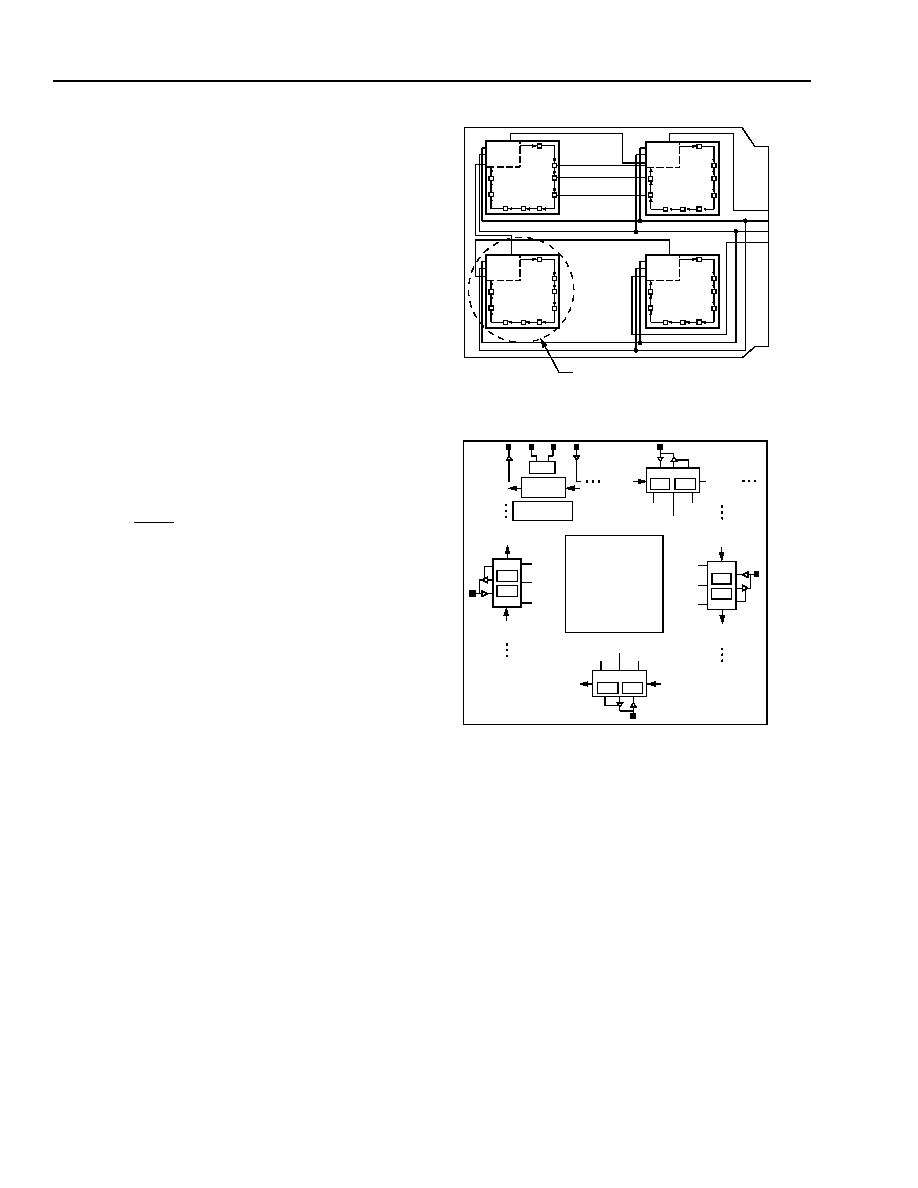
puts and examine inputs. In the configuration shown in
Figure 36, where boundary scan is used to test ICs,
test data is transmitted serially into TDI of the first
BSCAN device (U1), through TDO/TDI connections
between BSCAN devices (U2 and U3), and out TDO of
the last BSCAN device (U4). In this configuration, the
TMS and TCK signals are routed to all boundary-scan
ICs in parallel so that all boundary-scan components
operate in the same state. In other configurations, mul-
tiple scan paths are used instead of a single ring. When
multiple scan paths are used, each ring is indepen-
dently controlled by its own TMS and TCK signals.
Figure 37 provides a system interface for components
used in the boundary-scan testing of PCBs. The three
major components shown are the test host, boundary-
scan support circuit, and the devices under test
(DUTs). The DUTs shown here are
ORCA Series
FPGAs with dedicated boundary-scan circuitry. The
test host is normally one of the following: automatic test
equipment (ATE), a workstation, a PC, or a micropro-
cessor.
5-5972(F)
Key:
BSC = boundary-scan cell, BDC = bidirectional data cell,
and DCC = data control cell.
Figure 36. Printed-Circuit Board with Boundary-
Scan Circuitry
TDI
TMS
TCK
TDO
TDI
TDO
TMS
TCK
U2
net a
net b
net c
PLC
ARRAY
BDC
BSC
p_in
p_ts
SCAN
OUT
SCAN
IN
PR[ij]
DCC
p_out
BDC
BSC
p_in
p_out
p_ts
PL[ij]
DCC
SCAN
IN
SCAN
OUT
BDC
DCC
BSC
p_in
p_out
p_ts
SCAN
OUT
PB[ij]
SCAN
IN
TDO TCK TMS TDI
TAPC
BYPASS
REGISTER
INSTRUCTION
REGISTER
BDC
DCC
BSC
p_in
p_out
p_ts
SCAN
OUT
SCAN
IN
PT[ij]
SEE ENLARGED VIEW BELOW
s
TDI
TDO
TMS
TCK
U3
TDI
TDO
TMS
TCK
U4
TDI
TDO
TMS
TCK
U2
相关PDF资料 |
PDF描述 |
|---|---|
| OR3T80-4PS240I | FPGA, 484 CLBS, 58000 GATES, 80 MHz, PQFP240 |
| OR3T80-4PS240 | FPGA, 484 CLBS, 58000 GATES, 80 MHz, PQFP240 |
| OR3C80-4B432 | FPGA, 484 CLBS, 58000 GATES, PBGA432 |
| OR3C80-4B600 | FPGA, 484 CLBS, 58000 GATES, PBGA600 |
| OR3C80-5B432 | FPGA, 484 CLBS, 58000 GATES, PBGA432 |
相关代理商/技术参数 |
参数描述 |
|---|---|
| OR3T55-4PS240I | 制造商:未知厂家 制造商全称:未知厂家 功能描述:Field Programmable Gate Array (FPGA) |
| OR3T55-5BA256 | 制造商:AGERE 制造商全称:AGERE 功能描述:3C and 3T Field-Programmable Gate Arrays |
| OR3T55-5BA256I | 制造商:AGERE 制造商全称:AGERE 功能描述:3C and 3T Field-Programmable Gate Arrays |
| OR3T55-5BA352 | 制造商:AGERE 制造商全称:AGERE 功能描述:3C and 3T Field-Programmable Gate Arrays |
| OR3T55-5BA352I | 制造商:AGERE 制造商全称:AGERE 功能描述:3C and 3T Field-Programmable Gate Arrays |
发布紧急采购,3分钟左右您将得到回复。