- 您现在的位置:买卖IC网 > PDF目录296762 > P89LPC932A1FDH (NXP Semiconductors N.V.) 8-bit microcontroller with accelerated two-clock 80C51 core 8 kB 3 V byte-erasable flash with 512-byte data EEPROM PDF资料下载
参数资料
| 型号: | P89LPC932A1FDH |
| 厂商: | NXP Semiconductors N.V. |
| 元件分类: | 8位微控制器 |
| 英文描述: | 8-bit microcontroller with accelerated two-clock 80C51 core 8 kB 3 V byte-erasable flash with 512-byte data EEPROM |
| 封装: | P89LPC932A1FDH<SOT361-1 (TSSOP28)|<<http://www.nxp.com/packages/SOT361-1.html<1<week 47, 2004,;P89LPC932A1FDH/G<SOT361-1 (TSSOP28)|<<http://www.nxp.com/packages/SOT361-1. |
| 文件页数: | 10/64页 |
| 文件大小: | 319K |
| 代理商: | P89LPC932A1FDH |
第1页第2页第3页第4页第5页第6页第7页第8页第9页当前第10页第11页第12页第13页第14页第15页第16页第17页第18页第19页第20页第21页第22页第23页第24页第25页第26页第27页第28页第29页第30页第31页第32页第33页第34页第35页第36页第37页第38页第39页第40页第41页第42页第43页第44页第45页第46页第47页第48页第49页第50页第51页第52页第53页第54页第55页第56页第57页第58页第59页第60页第61页第62页第63页第64页
P89LPC932A1_3
NXP B.V. 2007. All rights reserved.
Product data sheet
Rev. 03 — 12 March 2007
18 of 64
NXP Semiconductors
P89LPC932A1
8-bit microcontroller with accelerated two-clock 80C51 core
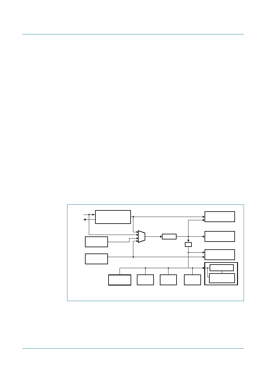
The frequency of this clock output is 1
2 that of the CCLK. If the clock output is not needed
in Idle mode, it may be turned off prior to entering Idle, saving additional power.
7.4 On-chip RC oscillator option
The P89LPC932A1 has a 6-bit TRIM register that can be used to tune the frequency of
the RC oscillator. During reset, the TRIM value is initialized to a factory preprogrammed
value to adjust the oscillator frequency to 7.373 MHz
± 1 % at room temperature.
End-user applications can write to the TRIM register to adjust the on-chip RC oscillator to
other frequencies.
7.5 Watchdog oscillator option
The watchdog has a separate oscillator which has a frequency of 400 kHz. This oscillator
can be used to save power when a high clock frequency is not needed.
7.6 External clock input option
In this conguration, the processor clock is derived from an external source driving the
P3.1/XTAL1 pin. The rate may be from 0 Hz up to 18 MHz. The P3.0/XTAL2 pin may be
used as a standard port pin or a clock output. When using an oscillator frequency
above 12 MHz, the reset input function of P1.5 must be enabled. An external circuit
is required to hold the device in reset at power-up until VDD has reached its
specied level. When system power is removed, VDD will fall below the minimum
specied operating voltage. When using an oscillator frequency above 12 MHz, in
some applications, an external brownout detect circuit may be required to hold the
device in reset when VDD falls below the minimum specied operating voltage.
Fig 7.
Block diagram of oscillator control
÷2
002aaa891
RTC
CPU
WDT
DIVM
CCLK
UART
OSCCLK
I2C-BUS
PCLK
TIMER 0 AND
TIMER 1
HIGH FREQUENCY
MEDIUM FREQUENCY
LOW FREQUENCY
XTAL1
XTAL2
RC
OSCILLATOR
WATCHDOG
OSCILLATOR
(7.3728 MHz
±1 %)
PCLK
RCCLK
SPI
CCU
(P89LPC932A1)
32
× PLL
+20%
30 %
(400 kHz
)
相关PDF资料 |
PDF描述 |
|---|---|
| P89LPC932A1FHN | 8-bit microcontroller with accelerated two-clock 80C51 core 8 kB 3 V byte-erasable flash with 512-byte data EEPROM |
| P89LPC9331FDH | 8-bit microcontroller with accelerated two-clock 80C51 core, 4 kB-8 kB-16 kB 3 V byte-erasable flash with 8-bit ADCs |
| P89LPC9331HDH | 8-bit microcontroller with accelerated two-clock 80C51 core, 4 kB-8 kB-16 kB 3 V byte-erasable flash with 8-bit ADCs |
| P89LPC9341FDH | 8-bit microcontroller with accelerated two-clock 80C51 core, 4 kB-8 kB-16 kB 3 V byte-erasable flash with 8-bit ADCs |
| P89LPC9351FDH | 8-bit microcontroller with accelerated two-clock 80C51 core, 4 kB-8 kB-16 kB 3 V byte-erasable flash with 8-bit ADCs |
相关代理商/技术参数 |
参数描述 |
|---|---|
| P89LPC932A1FDH,512 | 功能描述:8位微控制器 -MCU 80C51 8K FL 768B RAM RoHS:否 制造商:Silicon Labs 核心:8051 处理器系列:C8051F39x 数据总线宽度:8 bit 最大时钟频率:50 MHz 程序存储器大小:16 KB 数据 RAM 大小:1 KB 片上 ADC:Yes 工作电源电压:1.8 V to 3.6 V 工作温度范围:- 40 C to + 105 C 封装 / 箱体:QFN-20 安装风格:SMD/SMT |
| P89LPC932A1FDH,529 | 功能描述:8位微控制器 -MCU 8K FL/768B RAM/512B EE/CCU RoHS:否 制造商:Silicon Labs 核心:8051 处理器系列:C8051F39x 数据总线宽度:8 bit 最大时钟频率:50 MHz 程序存储器大小:16 KB 数据 RAM 大小:1 KB 片上 ADC:Yes 工作电源电压:1.8 V to 3.6 V 工作温度范围:- 40 C to + 105 C 封装 / 箱体:QFN-20 安装风格:SMD/SMT |
| P89LPC932A1FDH512 | 制造商:NXP Semiconductors 功能描述:IC 8BIT MCU 80C51 18MHZ TSSOP-28 |
| P89LPC932A1FHN | 制造商:NXP Semiconductors 功能描述:MCU 8BIT 80C51 8K FLASH HVQFN-28 |
| P89LPC932A1FHN,151 | 功能描述:8位微控制器 -MCU 80C51 8K FL 768B RAM RoHS:否 制造商:Silicon Labs 核心:8051 处理器系列:C8051F39x 数据总线宽度:8 bit 最大时钟频率:50 MHz 程序存储器大小:16 KB 数据 RAM 大小:1 KB 片上 ADC:Yes 工作电源电压:1.8 V to 3.6 V 工作温度范围:- 40 C to + 105 C 封装 / 箱体:QFN-20 安装风格:SMD/SMT |
发布紧急采购,3分钟左右您将得到回复。