- 您现在的位置:买卖IC网 > PDF目录296762 > P89LPC932A1FDH (NXP Semiconductors N.V.) 8-bit microcontroller with accelerated two-clock 80C51 core 8 kB 3 V byte-erasable flash with 512-byte data EEPROM PDF资料下载
参数资料
| 型号: | P89LPC932A1FDH |
| 厂商: | NXP Semiconductors N.V. |
| 元件分类: | 8位微控制器 |
| 英文描述: | 8-bit microcontroller with accelerated two-clock 80C51 core 8 kB 3 V byte-erasable flash with 512-byte data EEPROM |
| 封装: | P89LPC932A1FDH<SOT361-1 (TSSOP28)|<<http://www.nxp.com/packages/SOT361-1.html<1<week 47, 2004,;P89LPC932A1FDH/G<SOT361-1 (TSSOP28)|<<http://www.nxp.com/packages/SOT361-1. |
| 文件页数: | 62/64页 |
| 文件大小: | 319K |
| 代理商: | P89LPC932A1FDH |
第1页第2页第3页第4页第5页第6页第7页第8页第9页第10页第11页第12页第13页第14页第15页第16页第17页第18页第19页第20页第21页第22页第23页第24页第25页第26页第27页第28页第29页第30页第31页第32页第33页第34页第35页第36页第37页第38页第39页第40页第41页第42页第43页第44页第45页第46页第47页第48页第49页第50页第51页第52页第53页第54页第55页第56页第57页第58页第59页第60页第61页当前第62页第63页第64页
P89LPC932A1_3
NXP B.V. 2007. All rights reserved.
Product data sheet
Rev. 03 — 12 March 2007
7 of 64
NXP Semiconductors
P89LPC932A1
8-bit microcontroller with accelerated two-clock 80C51 core
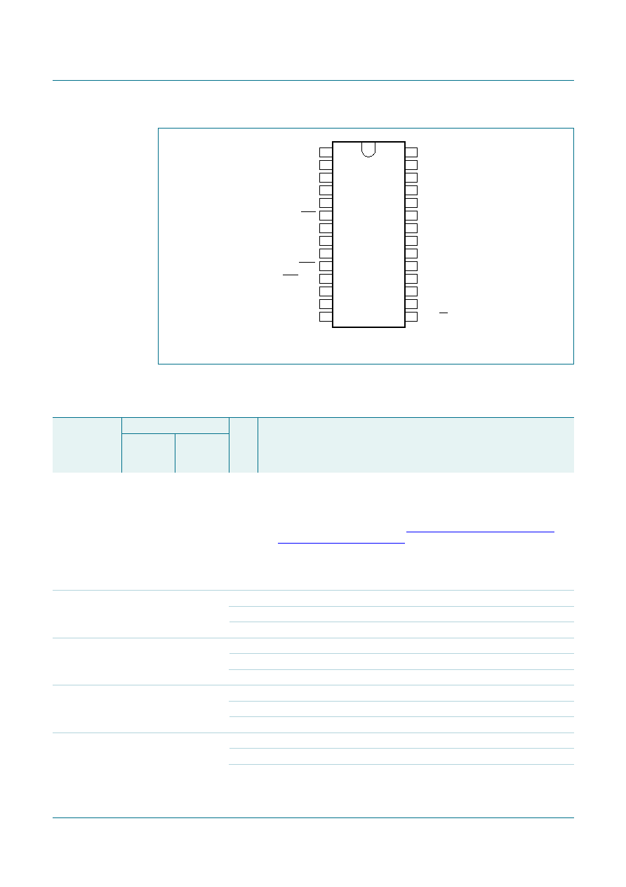
6.2 Pin description
Fig 6.
P89LPC932A1 DIP28 pin conguration
P89LPC932A1FN
002aac785
1
2
3
4
5
6
7
8
9
10
11
12
13
14
16
15
18
17
20
19
22
21
24
23
26
25
28
27
P2.0/ICB
P2.1/OCD
P0.0/CMP2/KBI0
P1.7/OCC
P1.6/OCB
P1.5/RST
VSS
P3.1/XTAL1
P3.0/XTAL2/CLKOUT
P1.4/INT1
P1.3/INT0/SDA
P1.2/T0/SCL
P2.2/MOSI
P2.3/MISO
P2.7/ICA
P2.6/OCA
P0.1/CIN2B/KBI1
P0.2/CIN2A/KBI2
P0.3/CIN1B/KBI3
P0.4/CIN1A/KBI4
P0.5/CMPREF/KBI5
VDD
P0.6/CMP1/KBI6
P0.7/T1/KBI7
P1.0/TXD
P1.1/RXD
P2.5/SPICLK
P2.4/SS
Table 2.
Pin description
Symbol
Pin
Type Description
TSSOP28,
PLCC28,
DIP28
HVQFN28
P0.0 to P0.7
I/O
Port 0: Port 0 is an 8-bit I/O port with a user-congurable output type.
During reset Port 0 latches are congured in the input only mode with the
internal pull-up disabled. The operation of Port 0 pins as inputs and
outputs depends upon the port conguration selected. Each port pin is
congured independently. Refer to Section 7.13.1 “Port congurations”
and Table 8 “Static characteristics” for details.
The Keypad Interrupt feature operates with Port 0 pins.
All pins have Schmitt trigger inputs.
Port 0 also provides various special functions as described below:
P0.0/CMP2/
KBI0
3
27
I/O
P0.0 — Port 0 bit 0.
O
CMP2 — Comparator 2 output.
I
KBI0 — Keyboard input 0.
P0.1/CIN2B/
KBI1
26
22
I/O
P0.1 — Port 0 bit 1.
I
CIN2B — Comparator 2 positive input B.
I
KBI1 — Keyboard input 1.
P0.2/CIN2A/
KBI2
25
21
I/O
P0.2 — Port 0 bit 2.
I
CIN2A — Comparator 2 positive input A.
I
KBI2 — Keyboard input 2.
P0.3/CIN1B/
KBI3
24
20
I/O
P0.3 — Port 0 bit 3.
I
CIN1B — Comparator 1 positive input B.
I
KBI3 — Keyboard input 3.
相关PDF资料 |
PDF描述 |
|---|---|
| P89LPC932A1FHN | 8-bit microcontroller with accelerated two-clock 80C51 core 8 kB 3 V byte-erasable flash with 512-byte data EEPROM |
| P89LPC9331FDH | 8-bit microcontroller with accelerated two-clock 80C51 core, 4 kB-8 kB-16 kB 3 V byte-erasable flash with 8-bit ADCs |
| P89LPC9331HDH | 8-bit microcontroller with accelerated two-clock 80C51 core, 4 kB-8 kB-16 kB 3 V byte-erasable flash with 8-bit ADCs |
| P89LPC9341FDH | 8-bit microcontroller with accelerated two-clock 80C51 core, 4 kB-8 kB-16 kB 3 V byte-erasable flash with 8-bit ADCs |
| P89LPC9351FDH | 8-bit microcontroller with accelerated two-clock 80C51 core, 4 kB-8 kB-16 kB 3 V byte-erasable flash with 8-bit ADCs |
相关代理商/技术参数 |
参数描述 |
|---|---|
| P89LPC932A1FDH,512 | 功能描述:8位微控制器 -MCU 80C51 8K FL 768B RAM RoHS:否 制造商:Silicon Labs 核心:8051 处理器系列:C8051F39x 数据总线宽度:8 bit 最大时钟频率:50 MHz 程序存储器大小:16 KB 数据 RAM 大小:1 KB 片上 ADC:Yes 工作电源电压:1.8 V to 3.6 V 工作温度范围:- 40 C to + 105 C 封装 / 箱体:QFN-20 安装风格:SMD/SMT |
| P89LPC932A1FDH,529 | 功能描述:8位微控制器 -MCU 8K FL/768B RAM/512B EE/CCU RoHS:否 制造商:Silicon Labs 核心:8051 处理器系列:C8051F39x 数据总线宽度:8 bit 最大时钟频率:50 MHz 程序存储器大小:16 KB 数据 RAM 大小:1 KB 片上 ADC:Yes 工作电源电压:1.8 V to 3.6 V 工作温度范围:- 40 C to + 105 C 封装 / 箱体:QFN-20 安装风格:SMD/SMT |
| P89LPC932A1FDH512 | 制造商:NXP Semiconductors 功能描述:IC 8BIT MCU 80C51 18MHZ TSSOP-28 |
| P89LPC932A1FHN | 制造商:NXP Semiconductors 功能描述:MCU 8BIT 80C51 8K FLASH HVQFN-28 |
| P89LPC932A1FHN,151 | 功能描述:8位微控制器 -MCU 80C51 8K FL 768B RAM RoHS:否 制造商:Silicon Labs 核心:8051 处理器系列:C8051F39x 数据总线宽度:8 bit 最大时钟频率:50 MHz 程序存储器大小:16 KB 数据 RAM 大小:1 KB 片上 ADC:Yes 工作电源电压:1.8 V to 3.6 V 工作温度范围:- 40 C to + 105 C 封装 / 箱体:QFN-20 安装风格:SMD/SMT |
发布紧急采购,3分钟左右您将得到回复。