- 您现在的位置:买卖IC网 > PDF目录296790 > PBA31301/2S (ERICSSON POWER MODULES AB) SPECIALTY TELECOM CIRCUIT, CBGA34 PDF资料下载
参数资料
| 型号: | PBA31301/2S |
| 厂商: | ERICSSON POWER MODULES AB |
| 元件分类: | 通信及网络 |
| 英文描述: | SPECIALTY TELECOM CIRCUIT, CBGA34 |
| 封装: | 10.20 X 14 X 1.60 MM, BGA-34 |
| 文件页数: | 10/12页 |
| 文件大小: | 812K |
| 代理商: | PBA31301/2S |
7
PBA 313 01
EN/LZT 146 65 R3B Ericsson Microelectronics AB, October 2001
TX_CLK
1 MHz transmit clock digital output available for the baseband
circuitry when the POR_EXT and SYS_CLK_REQ (see above)
are both 'high'. TX_CLK changes value on rising edges of
SYS_CLK.
LPO_CLK
3.2 kHz low power oscillator clock digital output that is
adjustable by setting the internal LPOHI and LPOLO registers
(see Design Considerations). The clock output is available
as soon as the power supply is applied and POR_EXT is
'high' (figure 7). The LPO is necessary for wake-up timing
in the baseband circuitry, if the Ericsson baseband is used.
LPO_CLK must be trimmed to 1/2 LSB from 3.2 kHz or cali-
brated within 230 ppm, using SYS_CLK or TX_CLK.
Data Interface
Two digital signals are used for data flow over the air inter-
face.
TX_DATA
Transmit data digital control is active 'high'12). The radio
module feeds Bluetooth data (1Mbit/s) directly to the radio
frequency modulator when PHD_OFF is activated. The total
delay from the TX_DATA pin to the ANT pin is typically
0.5s.
RX_DATA
Receive data digital output is active 'high'. The radio module
latches out Bluetooth data (1 Mbit/s) on the RX_DATA pin on
each falling edge of SYS_CLK when RX_ON is activated. The
total delay from the ANT pin to the RX_DATA pin is typically
2.5s.
PHD_OFF
Phase detector off control is active 'high'. Activate this signal
in transmit mode to open the phase locked loop (PLL)
employed in the VCO synthesizer section and enable modula-
tion of the carrier using the TX_DATA digital input. PHD_OFF
is activated after the initialization of the SYNT_ON signal and
the TX_ON signal, see figure 6 and table 2.
POR_EXT
External power on reset is active 'high'. An external power-
on-reset digital input signal that will reset the radio controller
and its registers. A reset will occur on the positive edge of
POR_EXT signal.
SYS_CLK_REQ
System clock request control is active 'high'. Once the crystal
oscillator bit (XOCTR, control register, bit #2) has been set,
use this control to switch off (sleep mode) and wake up
(idle and operating modes) the reference clock circuitry and
corresponding 13MHz and 1MHz clock output ports of the
module.
Output Control
There are four digital output control signals available for con-
trolling external baseband circuitry.
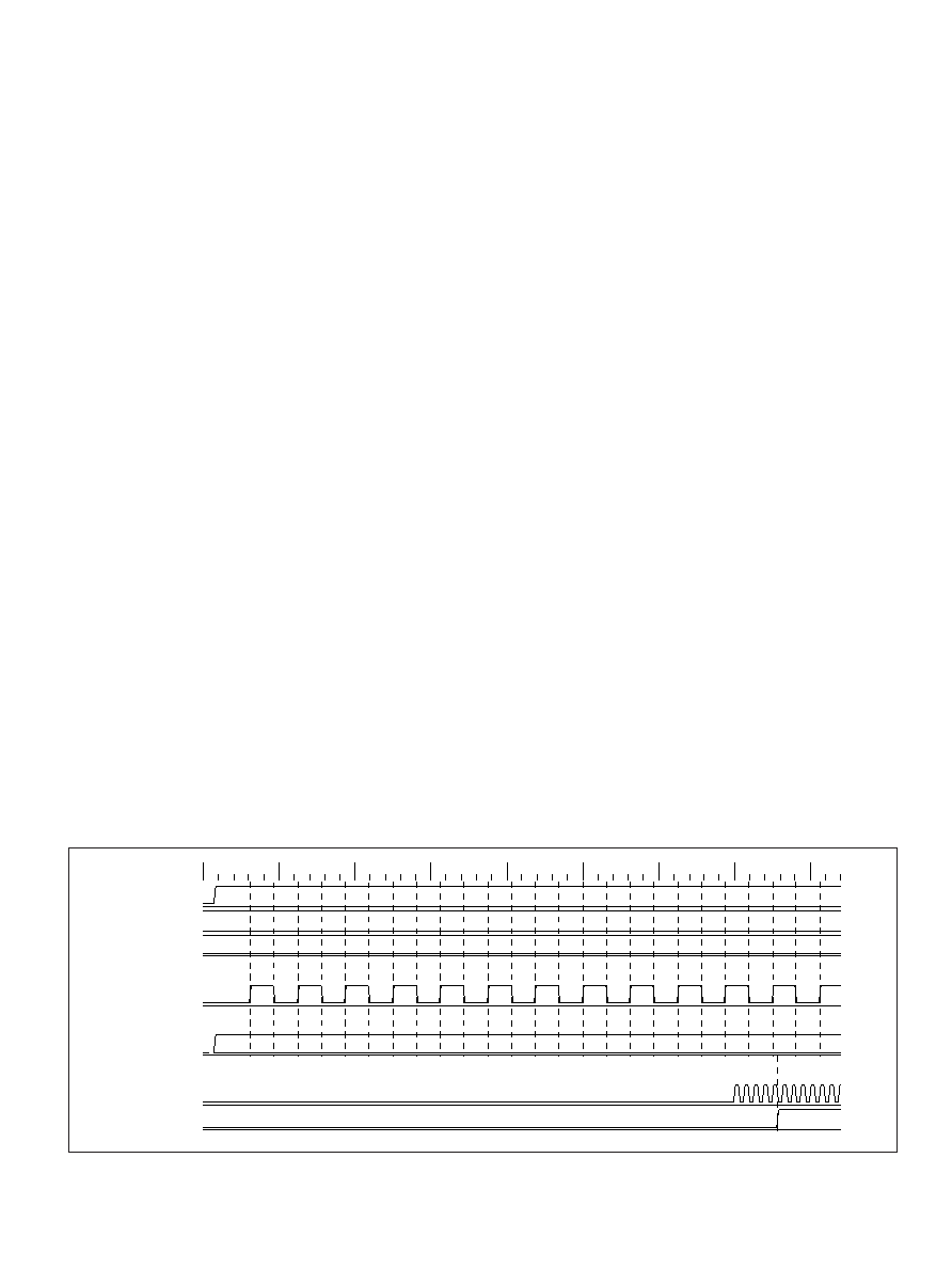
POR
Power-on-reset digital output is activated after the power has
been applied to the Bluetooth radio or on a positive edge of
the POR_EXT digital input. POR has a transition from 'low'
to 'high' after four clock cycles have been delivered to the
baseband chip, see figure 7.
SYS_CLK
13 MHz system clock digital output available for the base-
band circuitry when the POR_EXT and SYS_CLK_REQ are
both 'high'. SYS_CLK will also be available during startup,
independent on the value of SYS_CLK_REQ, see figure 7.
0
0.5ms
1.0ms
1.5ms
2.0ms
2.5ms
3.0ms
3.5ms
4.0ms
VCC
POR_EXT
SYS_CLK_REQ
LPO_CLK
Control
Register
SYS_CLK
POR
Vcc
’1’
’0’ or ’1 ’
10000XX
Figure 7. Powering up the module.
12) Data on the TX_DATA pin is digitally buffered before it is fed to the radio
frequency modulator. The polarity of this input can be set to normal by
writing ‘1’ or inverted by writing ‘0’ to bit 0 of the Enable register.
相关PDF资料 |
PDF描述 |
|---|---|
| PBA31301/2S | SPECIALTY TELECOM CIRCUIT, PBGA34 |
| PBA31301/3S | SPECIALTY TELECOM CIRCUIT, PBGA34 |
| PBA31301/3S | SPECIALTY TELECOM CIRCUIT, CBGA34 |
| PBL38773/1ML | TELECOM-SLIC, PQCC32 |
| PBL38773/1SO | TELECOM-SLIC, PDSO28 |
相关代理商/技术参数 |
参数描述 |
|---|---|
| PBA31302 | 制造商:INFINEON 制造商全称:Infineon Technologies AG 功能描述:Bluetooth Radio Transceiver |
| PBA31304 | 制造商:未知厂家 制造商全称:未知厂家 功能描述:Telecomm/Datacomm |
| PBA31305 | 制造商:INFINEON 制造商全称:Infineon Technologies AG 功能描述:Bluetooth Radio Transceiver |
| PBA31307 | 制造商:INFINEON 制造商全称:Infineon Technologies AG 功能描述:SINGLE STONE |
| PBA31307/1R2AT | 功能描述:MODULE BLUETOOTH SINGLESTONE RoHS:否 类别:RF/IF 和 RFID >> RF 收发器 系列:- 产品培训模块:Lead (SnPb) Finish for COTS Obsolescence Mitigation Program 标准包装:30 系列:- 频率:4.9GHz ~ 5.9GHz 数据传输率 - 最大:54Mbps 调制或协议:* 应用:* 功率 - 输出:-3dBm 灵敏度:- 电源电压:2.7 V ~ 3.6 V 电流 - 接收:* 电流 - 传输:* 数据接口:PCB,表面贴装 存储容量:- 天线连接器:PCB,表面贴装 工作温度:-25°C ~ 85°C 封装/外壳:68-TQFN 裸露焊盘 包装:管件 |
发布紧急采购,3分钟左右您将得到回复。