- 您现在的位置:买卖IC网 > PDF目录296790 > PBA31301/2S (ERICSSON POWER MODULES AB) SPECIALTY TELECOM CIRCUIT, CBGA34 PDF资料下载
参数资料
| 型号: | PBA31301/2S |
| 厂商: | ERICSSON POWER MODULES AB |
| 元件分类: | 通信及网络 |
| 英文描述: | SPECIALTY TELECOM CIRCUIT, CBGA34 |
| 封装: | 10.20 X 14 X 1.60 MM, BGA-34 |
| 文件页数: | 7/12页 |
| 文件大小: | 812K |
| 代理商: | PBA31301/2S |
4
PBA 313 01
EN/LZT 146 65 R3B Ericsson Microelectronics AB, October 2001
Parameter
Condition
Symbol
Min
Typ
Max
Unit
Transmitter Performance
Frequency modulation
Deviation from
fMod
140
155
175
kHz
center frequency9)
Initial frequency error
10)
-75
0
+75
kHz
TX power
-4
4.5
dBm
TX carrier drift
1 slot (366 s)
fDrift1
-25
25
kHz
3 slots (1598 s)
fDrift2
-40
40
kHz
5 slots (2862 s)
fDrift3
-40
40
kHz
20 dB bandwidth
Measured with RBW: 10 kHz and peak detector
600
1000
kHz
Spurious Emissions
30 MHz – 1GHz
-36
dBm
1 GHz – 12.75 GHz
-30
dBm
1.8 GHz – 1.9 GHz
-47
dBm
5.15 GHz – 5.3 GHz
-47
dBm
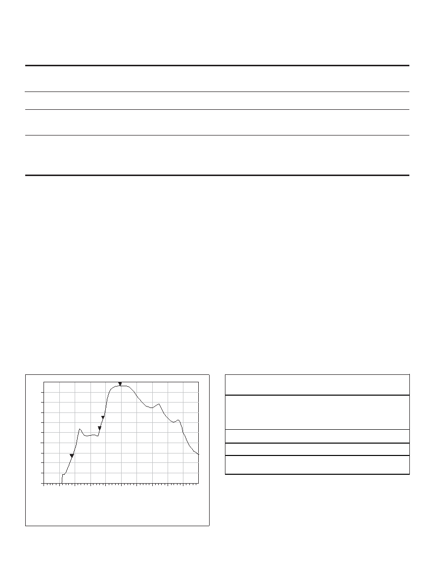
Figure 3. Blocking examples.
C/I Blocking
The blocking characteristics can be basically split into two
regions: In-band and Out-of-band. Blocking is performed
both on the chip and on the module level.
Out-of-band
– Antenna filter, DC to 1.9 GHz and 3:rd harmonic.
- Switch, low freq. and 2:nd harmonic.
- RX-balun, low freq. and 2:nd harmonic.
- On-chip IF filter.
RF Specifications, cont.
Figure 2 shows the combination blocking effect of the
antenna switch, antenna filter and RX balun. In addition to the
blocking characteristics shown in figure 2, there is antenna
isolation and filtering on the chip. Marker 1 shows the region
where the Bluetooth band is located. Markers 2 - 4 show the
blocking at the telecom frequency bands.
An example of total blocking characteristics can be seen in
figure 3.
Figure 2. Typical out-of-band blocking characteristics excluding
antenna isolation and on chip filtering.
Example 2
Interferenc e of +33 dBm a t 1910 MHz.
Antenna isolation
25 dB
Antenna filter,
36 dB
Antenna switch,
RX-balun
Interference level before
IF filter +33-25-36=
-28 dBm
0.1% BER carrier
level -40 + (-28)=
-68 dBm
Example 1
Interferenc e of +33 dBm a t 2015 MHz.
Antenna isolation
15 dB
Antenna filter,
27 dB
Antenna switch,
RX-balun
Interference level before
IF filter +33-15-27=
-9 dBm
0.1% BER carrier
level -40 + (-9)=
-49 dBm
0.1% BER requires a C/I of more than -40 dB at the IF filter.
9) fMod = (FMod1-FMod0)/2.
10) The initial frequency is mainly affected by the tolerance of the reference frequency or crystal; for every 1Hz deviation from 12MHz, the TX carrier offset is
altered by approximately 186Hz.
0.0
0.5
1.0
1.5
2.0
2.5
3.0
3.5
4.0
4.5
5.0
GHz
-100
-90
-80
-70
-60
-50
-40
-30
-20
-10
0
m1
freq=2.450GHz
dB( RX path)=
m1
m2
freq=900.0MHz
dB(RX path) =
m2
m3
freq=1.800GHz
=
m3
m4
freq=1.900GHz
) =
m4
dB(RX
path)
dB(RX path)
dB(RX path
-3.529
-74.58
-47.426
-36.537
相关PDF资料 |
PDF描述 |
|---|---|
| PBA31301/2S | SPECIALTY TELECOM CIRCUIT, PBGA34 |
| PBA31301/3S | SPECIALTY TELECOM CIRCUIT, PBGA34 |
| PBA31301/3S | SPECIALTY TELECOM CIRCUIT, CBGA34 |
| PBL38773/1ML | TELECOM-SLIC, PQCC32 |
| PBL38773/1SO | TELECOM-SLIC, PDSO28 |
相关代理商/技术参数 |
参数描述 |
|---|---|
| PBA31302 | 制造商:INFINEON 制造商全称:Infineon Technologies AG 功能描述:Bluetooth Radio Transceiver |
| PBA31304 | 制造商:未知厂家 制造商全称:未知厂家 功能描述:Telecomm/Datacomm |
| PBA31305 | 制造商:INFINEON 制造商全称:Infineon Technologies AG 功能描述:Bluetooth Radio Transceiver |
| PBA31307 | 制造商:INFINEON 制造商全称:Infineon Technologies AG 功能描述:SINGLE STONE |
| PBA31307/1R2AT | 功能描述:MODULE BLUETOOTH SINGLESTONE RoHS:否 类别:RF/IF 和 RFID >> RF 收发器 系列:- 产品培训模块:Lead (SnPb) Finish for COTS Obsolescence Mitigation Program 标准包装:30 系列:- 频率:4.9GHz ~ 5.9GHz 数据传输率 - 最大:54Mbps 调制或协议:* 应用:* 功率 - 输出:-3dBm 灵敏度:- 电源电压:2.7 V ~ 3.6 V 电流 - 接收:* 电流 - 传输:* 数据接口:PCB,表面贴装 存储容量:- 天线连接器:PCB,表面贴装 工作温度:-25°C ~ 85°C 封装/外壳:68-TQFN 裸露焊盘 包装:管件 |
发布紧急采购,3分钟左右您将得到回复。