- 您现在的位置:买卖IC网 > PDF目录378041 > PBL386652QNS (ERICSSON) Subscriber Line Interface Circuit PDF资料下载
参数资料
| 型号: | PBL386652QNS |
| 厂商: | ERICSSON |
| 英文描述: | Subscriber Line Interface Circuit |
| 中文描述: | 用户线接口电路 |
| 文件页数: | 14/18页 |
| 文件大小: | 184K |
| 代理商: | PBL386652QNS |
PBL 386 65/2
14
Preliminary
Active- to Reversal-state and Reversal-
to Active state and the setup time use
following formulas.
Active
→
Reversal:
t
Act
→
Rev =
C
SPR
.
17500
Reversal
→
Active:
t
Rev
→
Act =
C
SPR
.
15500
The time is measured between 10%
and 90% of the line voltage. The reversal
time is independent of line load and line
current.
Analog Temperature Guard
The widely varying environmental condi-
tions in which SLICs operate may lead to
the chip temperature limitations being ex-
ceeded. The PBL 386 65/2 SLIC reduces
the dc line current and the longitudinal
current limit when the chip temperature
reaches approximately 145
°
C and increas-
es it again automatically when the temper-
ature drops.
The detector output, DET, is forced to a
logic low level when the temperature guard
is active.
Loop Monitoring Functions
The loop current, ground key and ring trip
detectors report their status through a com-
mon output, DET. The status of the detec-
tor pin, DET, is selected via the three bit
control interface C1, C2 and C3. Please
refer to section Control Inputs for a descrip-
tion of the control interface.
Loop Current Detector
The loop current detector indicates that the
telephone is off hook and that DC current is
flowing in the loop by putting the output pin
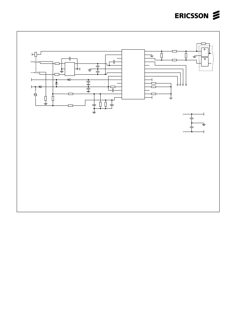
RESISTORS: (Values according to IEC-63 E96
series)
R
SG
R
LD
R
LC
R
REF
R
T
R
TX
R
B
R
RX
R
FB
R
1
R
2
R
3
R
4
R
RT
R
RF
R
F1
, R
F2
= 23.7 k
= 49.9 k
= 18.7 k
= 15 k
= 105 k
= 32.4k
= 57.6k
= 105k
Depending on CODEC / filter
= 604 k
1%
1
/
10
W
= 604 k
1%
1
/
10
W
= 249 k
1%
1
/
10
W
= 280 k
1%
1
/
W
= 332
5% 2 W
= 332
5% 2 W
= Line resistor, 40
1%
1%
1
/
10
W
1%
1
/
10
W
1%
1
/
10
W
1%
1
/
10
W
1%
1
/
10
W
1%
1
/
10
W
1%
1
/
10
W
1%
1
/
W
CAPACITORS:(Values according to IEC-63 E6
series)
C
B
C
B2
C
VCC
C
VEE
C
TC
C
RC
C
HP
C
LP
C
GG
C
1
C
2
= 100 nF
= 150 nF
= 100 nF
= 100 nF
= 1 nF
= 1 nF
= 68 nF
= 330 nF
= 220 nF
= 330 nF
= 330 nF
100 V 20%
100 V 20%
10 V 20%
10 V* 20%
100 V 20%
100 V 20%
100 V 20%
100 V 20%
100 V 20%
63 V 10%
63 V 10%
*100V if VEE pin connected to VBAT, VBAT2
Figure 13. Single-channel subscriber line interface with PBL 386 65/2 and combination CODEC/filter
DIODES:
D
B
D
B2
D
BB
= 1N4448
= 1N4448
= 1N4448 (optional)
OVP:
Secondary protection (eg Power Innovations TISP
PBL2). The ground terminals of the secondary
protection should be connected to the common
ground on the Printed Board Assembly with a track
as short and wide as possible, preferably a
groundplane.
C
VCC
CODEC/
Filter
SYSTEM CONTROL
INTERFACE
D
B2
C
RC
C
LP
C
HP
TIP
RING
OVP
+12 V /+5V
C
1
R
4
E
RG
R
RT
R
T
KR
VB
VB2
VCC
VCC
C
GG
C
2
R
3
C
TC
D
B
VEE
VEE
BGND
TIPX
VBAT
VBAT2
C1
C2
C3
VCC
AOV
PSG
LP
DR
PLD
PLC
SPR
REF
TS
NC
HP
RINGX
AGND
RSN
DET
NC
RRLY
VTX
DT
VEE
R
FB
R
RX
R
B
R
LD
R
LC
R
REF
R
F1
R
F2
R
1
R
2
R
SG
D
BB
C
B2
PBL 386 65/2
VB
R
TX
VBAT<VEE<-5 V
out
-
+
out
C
VEE
R
RF
+5 V
C
B
相关PDF资料 |
PDF描述 |
|---|---|
| PBL386652QNT | Subscriber Line Interface Circuit |
| PBL38665-2 | Subscriber Line Interface Circuit |
| PBL386652 | Subscriber Line Interface Circuit |
| PBL386652SHT | Subscriber Line Interface Circuit |
| PBL388121SOT | Voice-switch circuit for Handsfree speakerphone TAM |
相关代理商/技术参数 |
参数描述 |
|---|---|
| PBL386652QNT | 制造商:ERICSSON 制造商全称:Ericsson 功能描述:Subscriber Line Interface Circuit |
| PBL386652SHT | 制造商:ERICSSON 制造商全称:Ericsson 功能描述:Subscriber Line Interface Circuit |
| PBL38780/1QSD | 制造商:Rochester Electronics LLC 功能描述:- Bulk |
| PBL387821QSD | 制造商:Rochester Electronics LLC 功能描述:- Bulk 制造商:Infineon Technologies AG 功能描述: |
| PBL38812 | 制造商:ERICSSON 制造商全称:Ericsson 功能描述:Voice-switch circuit for Handsfree speakerphone TAM |
发布紧急采购,3分钟左右您将得到回复。