- 您现在的位置:买卖IC网 > PDF目录3775 > PCA9505DGG,112 (NXP Semiconductors)IC I/O EXPANDER I2C 40B 56TSSOP PDF资料下载
参数资料
| 型号: | PCA9505DGG,112 |
| 厂商: | NXP Semiconductors |
| 文件页数: | 9/34页 |
| 文件大小: | 0K |
| 描述: | IC I/O EXPANDER I2C 40B 56TSSOP |
| 产品培训模块: | I²C Bus Fundamentals |
| 特色产品: | NXP - I2C Interface |
| 标准包装: | 35 |
| 接口: | I²C |
| 输入/输出数: | 40 |
| 中断输出: | 是 |
| 频率 - 时钟: | 400kHz |
| 电源电压: | 2.3 V ~ 5.5 V |
| 工作温度: | -40°C ~ 85°C |
| 安装类型: | 表面贴装 |
| 封装/外壳: | 56-TFSOP(0.240",6.10mm 宽) |
| 供应商设备封装: | 56-TSSOP |
| 包装: | 管件 |
| 包括: | POR |
| 产品目录页面: | 824 (CN2011-ZH PDF) |
| 其它名称: | 568-4244-5 935284486112 PCA9505DGG |
第1页第2页第3页第4页第5页第6页第7页第8页当前第9页第10页第11页第12页第13页第14页第15页第16页第17页第18页第19页第20页第21页第22页第23页第24页第25页第26页第27页第28页第29页第30页第31页第32页第33页第34页
xxxxxxxxxxxxxxxxxxxxx xxxxxxxxxxxxxxxxxxxxxxxxxx xxxxxxx x x x xxxxxxxxxxxxxxxxxxxxxxxxxxxxxx xxxxxxxxxxxxxxxxxxx xx xx xxxxx
xxxxxxxxxxxxxxxxxxxxxxxxxxx xxxxxxxxxxxxxxxxxxx xxxxxx xxxxxxxxxxxxxxxxxxxxxxxxxxxxxxxxxxx xxxxxxxxxxxx x x
xxxxxxxxxxxxxxxxxxxxx xxxxxxxxxxxxxxxxxxxxxxxxxxxxxx xxxxx xxxxxxxxxxxxxxxxxxxxxxxxxxxxxxxxxxxxxxxxxxxxxxxxxx xxxxxxxx
xxxxxxxxxxxxxxxxxxxxxxxxx xxxxxxxxxxxxxxxxxxxx xxx
PCA
950
5_950
6
A
lli
n
for
m
at
ion
pr
ovi
ded
in
this
do
cum
ent
i
s
sub
jec
tto
leg
a
ld
is
c
la
im
er
s.
NXP
B.V
.
2010.
Al
lr
ig
h
ts
re
s
e
rv
ed.
Produ
ct
d
a
ta
sheet
Rev
.4
—
3
A
ugu
st
2
010
17
o
f34
N
X
P
Semi
conductor
s
PCA9505/06
40
-bit
I
2C-bus
I/O
port
with
RESET
,O
E
and
INT
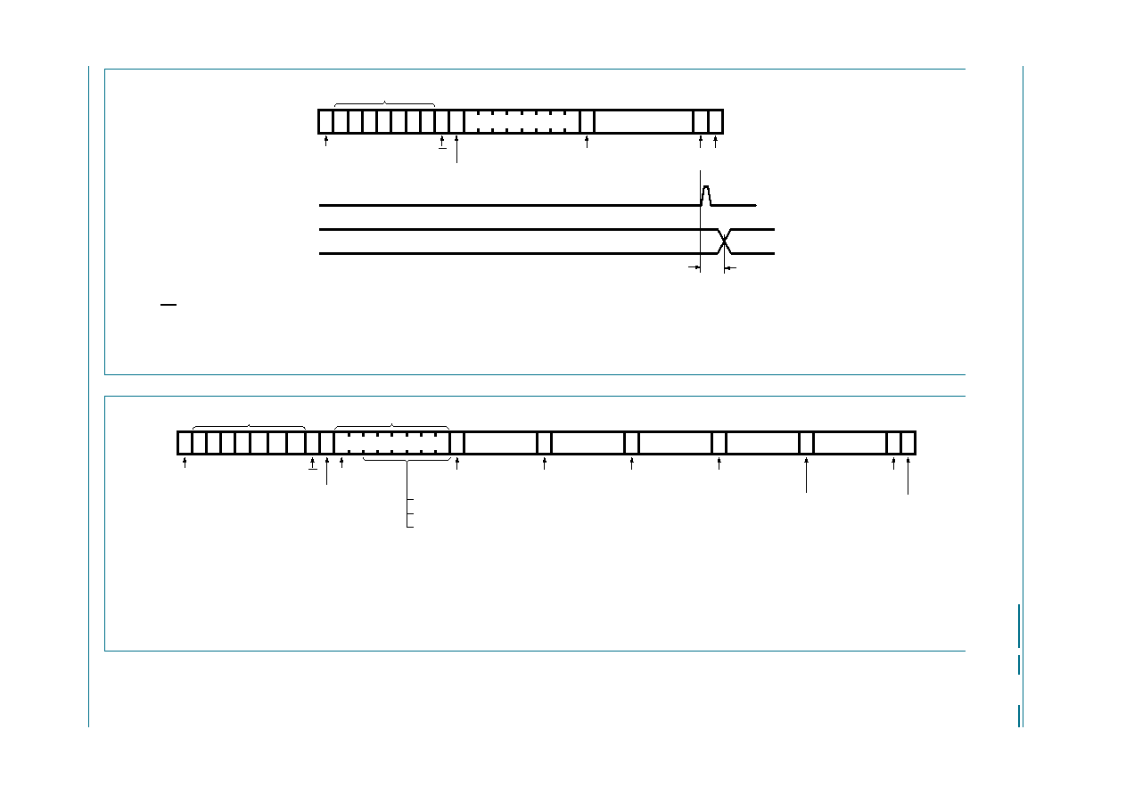
OE is LOW to observe a change in the outputs.
Two, three, or four adjacent banks can be programmed by using the Auto-Increment feature (AI = 1) and change at the corresponding output port becomes effective at
each acknowledge.
Fig 12. Write to a specific output port
002aab497
0
1
0
0 A2 A1 A0 0
slave address
R/W
S
START condition
SDA
A
acknowledge
from slave
AI 0001 D2 D1 D0 A
acknowledge
from slave
DATA BANK X
A
acknowledge
from slave
P
STOP
condition
A
write to port
data out from port
tv(Q)
data X
valid
The programming becomes effective at the acknowledge.
Less than 5 bytes can be programmed by using this scheme. D5, D4, D3, D2, D1, D0 refers to the first register to be programmed.
If more than 5 bytes are written, previous data are overwritten (the sixth Configuration register will roll over to the first addressed Configuration register, the sixth Polarity
Inversion register will roll over to the first addressed Polarity Inversion register and the sixth Mask Interrupt register will roll over to the first addressed Mask Interrupt
register).
Fig 13. Write to the I/O Configuration, Polarity Inversion or Mask Interrupt registers
002aab498
0
1
0
0 A2 A1 A0 0
slave address
R/W
S
START condition
SDA
A
acknowledge
from slave
1
0 D5 D4 D3 D2 D1 D0
command register
AI = 1
A
acknowledge
from slave
DATA BANK 0
A
DATA BANK 1
A
DATA BANK 2
A
DATA BANK 3
P
STOP
condition
A
acknowledge
from slave
DATA BANK 4
A
acknowledge
from slave
acknowledge
from slave
D[5:0] = 01 0000 for Polarity Inversion register programming bank 0
D[5:0] = 01 1000 for Configuration register programming bank 0
acknowledge
from slave
acknowledge
from slave
D[5:0] = 10 0000 for Mask Interrupt register programming bank 0
相关PDF资料 |
PDF描述 |
|---|---|
| ATTINY13-20MUR | IC MCU AVR 1K FLASH 10MHZ 20MLF |
| 5-530520-1 | CONT.HIGH CURRENT L.P. |
| 5-583875-6 | TWIN LEAF CONTACT |
| ATTINY861A-SUR | MCU AVR 8KB FLASH 20MHZ 20SOIC |
| 5-66067-5 | CONT AMP LEAF L/P 15 AU/100 SN |
相关代理商/技术参数 |
参数描述 |
|---|---|
| PCA9506 | 制造商:PHILIPS 制造商全称:NXP Semiconductors 功能描述:40-bit I2C-bus I/O port with RESET, OE and INT |
| PCA9506BS | 制造商:PHILIPS 制造商全称:NXP Semiconductors 功能描述:40-bit I2C-bus I/O port with RESET, OE and INT |
| PCA9506BS,118 | 功能描述:接口-I/O扩展器 I/O EXPANDER I2C RoHS:否 制造商:NXP Semiconductors 逻辑系列: 输入/输出端数量: 最大工作频率:100 kHz 工作电源电压:1.65 V to 5.5 V 工作温度范围:- 40 C to + 85 C 安装风格:SMD/SMT 封装 / 箱体:HVQFN-16 封装:Reel |
| PCA9506BS,118-CUT TAPE | 制造商:NXP 功能描述:PCA9506 Series 40-Bit I2C-Bus I/O Port with RESET OE and INT - HVQFN - 56 |
| PCA9506DGG | 功能描述:接口-I/O扩展器 I/O EXPANDER I2C RoHS:否 制造商:NXP Semiconductors 逻辑系列: 输入/输出端数量: 最大工作频率:100 kHz 工作电源电压:1.65 V to 5.5 V 工作温度范围:- 40 C to + 85 C 安装风格:SMD/SMT 封装 / 箱体:HVQFN-16 封装:Reel |
发布紧急采购,3分钟左右您将得到回复。