参数资料
| 型号: | PCA9535EMTTXG |
| 厂商: | ON Semiconductor |
| 文件页数: | 3/20页 |
| 文件大小: | 0K |
| 描述: | 16-BIT I/O EXPANDER |
| 标准包装: | 3,000 |
| 接口: | I²C 总线,SM 总线 |
| 输入/输出数: | 16 |
| 中断输出: | 是 |
| 频率 - 时钟: | 100kHz |
| 电源电压: | 1.65 V ~ 5.5 V |
| 工作温度: | -55°C ~ 125°C |
| 安装类型: | 表面贴装 |
| 封装/外壳: | 24-WFQFN 裸露焊盘 |
| 供应商设备封装: | 24-QFN(4x4) |
| 包装: | 带卷 (TR) |
| 包括: | * |
PCA9535E, PCA9535EC
http://onsemi.com
11
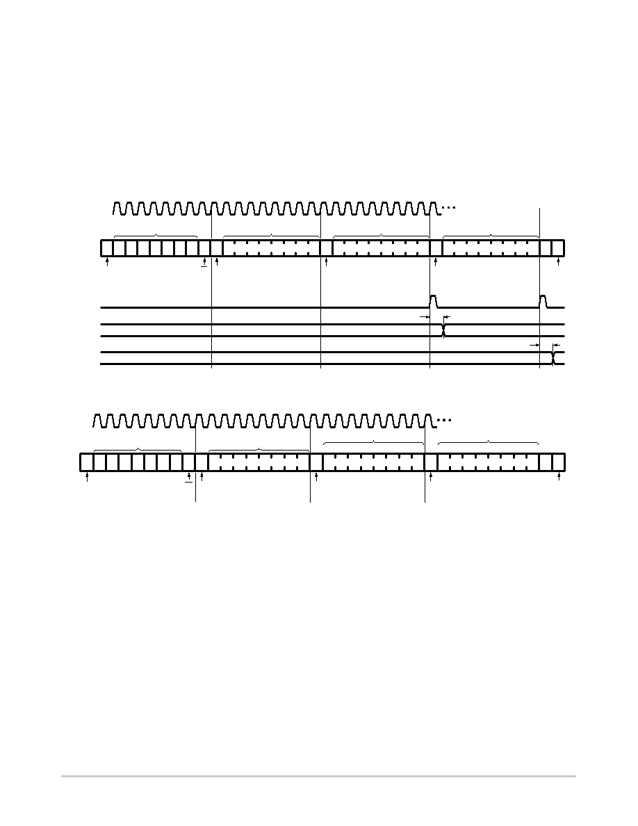
BUS TRANSACTIONS
Writing to the Port Registers
To transmit data to the PCA9535E/PCA9535EC, the bus
master must first send the device address with the least
significant bit set to logic 0 (see Figure 5 “PCA9535E and
PCA9535EC device address”). The command byte is sent
after the address and determines which registers will receive
the data following the command byte.
There
are
eight
registers
within
the
PCA9535E/PCA9535EC. These registers are configured to
operate as four register pairs: Input Ports, Output Ports,
Polarity Inversion Ports, and Configuration Ports. Data
bytes are sent alternately to each register in a register pair
Output Port 1 (register 3), then the next byte will be stored
in Output Port 0 (register 2). There is no limitation on the
number of data bytes sent in one write transmission. In this
way, each 8bit register may be updated independently of
the other registers.
Figure 6. Write to Output Port Registers
A2 A1 A0 0 A
S A6
START condition
R/W acknowledge
from slave
A
SCL
SDA
A
write to port
data out
from port 0
P
tv(Q)
9
8
7
6
5
4
3
2
1
command byte
data to port 0
DATA 0
slave address
0
STOP
condition
0.0
0.7
acknowledge
from slave
acknowledge
from slave
data to port 1
DATA 1
1.0
1.7
A
data out
from port 1
tv(Q)
DATA VALID
A5 A4 A3
0 0 0 0 0 1 0
Figure 7. Write to Configuration Registers
A2 A1 A0 0 A
S A6
START condition
R/W acknowledge
from slave
A
SCL
SDA
AP
9
8
7
6
5
4
3
2
1
command byte
data to register
DATA 0
slave address
0
STOP
condition
LSB
MSB
acknowledge
from slave
acknowledge
from slave
data to register
DATA 1
LSB
MSB
A
A5 A4 A3
0 0 0
1 1 0
0
Reading the Port Registers
To read data from the PCA9535E/PCA9535EC, the bus
master must first send the PCA9535E/PCA9535EC address
with the least significant bit set to logic 0 (see Figure 5
“PCA9535E and PCA9535EC device address”). The
command byte is sent after the address and determines
which register will be accessed.
After a restart, the device address must be sent again, but
this time, the least significant bit is set to logic 1. Data from
the register defined by the command byte will then be sent
Data is clocked into the register on the falling edge of the
acknowledge clock pulse. After the first byte is read,
additional bytes may be read but with data alternately
coming from each register in the pair. For example, if you
read Input Port 1, then the next byte read would be
Input Port 0. There is no limitation on the number of data
bytes received in one read transmission but the bus master
must not acknowledge the data for the final byte received.
相关PDF资料 |
PDF描述 |
|---|---|
| JLC1562BFEL | IC BUS INTRFACE I2C I/O 16SOEIAJ |
| ATMEGA8515-16JUR | MCU AVR 8KB FLASH 16MHZ 44PLCC |
| PCA9555D/G-T | IC I/O EXPANDER I2C 16B 24SOIC |
| ATMEGA48-15AZV | MCU AVR 4K FLASH 15MHZ 32-TQFP |
| ATMEGA48-15AZ | MCU AVR 4K FLASH 15MHZ 32-TQFP |
相关代理商/技术参数 |
参数描述 |
|---|---|
| PCA9535HF | 制造商:PHILIPS 制造商全称:NXP Semiconductors 功能描述:16-bit I2C-bus and SMBus, low power I/O port with interrupt |
| PCA9535HF,118 | 功能描述:I2C 接口集成电路 16BIT I2C FM TP GPIO RoHS:否 制造商:NXP Semiconductors 电源电压-最大:5.5 V 电源电压-最小:2.3 V 最大工作频率:400 KHz 最大工作温度:+ 85 C 封装 / 箱体:TSSOP-16 |
| PCA9535HF-T | 功能描述:I2C 接口集成电路 16BIT I2C FM TP GPIO INT RoHS:否 制造商:NXP Semiconductors 电源电压-最大:5.5 V 电源电压-最小:2.3 V 最大工作频率:400 KHz 最大工作温度:+ 85 C 封装 / 箱体:TSSOP-16 |
| PCA9535PW | 功能描述:I2C 接口集成电路 I2C/SMBUS 16BIT GPIO RoHS:否 制造商:NXP Semiconductors 电源电压-最大:5.5 V 电源电压-最小:2.3 V 最大工作频率:400 KHz 最大工作温度:+ 85 C 封装 / 箱体:TSSOP-16 |
| PCA9535PW,112 | 功能描述:I2C 接口集成电路 I2C/SMBUS 16BIT GPIO RoHS:否 制造商:NXP Semiconductors 电源电压-最大:5.5 V 电源电压-最小:2.3 V 最大工作频率:400 KHz 最大工作温度:+ 85 C 封装 / 箱体:TSSOP-16 |
发布紧急采购,3分钟左右您将得到回复。