- 您现在的位置:买卖IC网 > PDF目录3790 > PCF51JM64EVLK (Freescale Semiconductor)MCU 32BIT 64K FLASH 80-LQFP PDF资料下载
参数资料
| 型号: | PCF51JM64EVLK |
| 厂商: | Freescale Semiconductor |
| 文件页数: | 20/49页 |
| 文件大小: | 0K |
| 描述: | MCU 32BIT 64K FLASH 80-LQFP |
| 标准包装: | 90 |
| 系列: | MCF51JM |
| 核心处理器: | Coldfire V1 |
| 芯体尺寸: | 32-位 |
| 速度: | 50MHz |
| 连通性: | CAN,I²C,SCI,SPI,USB OTG |
| 外围设备: | LVD,PWM,WDT |
| 输入/输出数: | 66 |
| 程序存储器容量: | 64KB(64K x 8) |
| 程序存储器类型: | 闪存 |
| RAM 容量: | 16K x 8 |
| 电压 - 电源 (Vcc/Vdd): | 2.7 V ~ 5.5 V |
| 数据转换器: | A/D 12x12b |
| 振荡器型: | 外部 |
| 工作温度: | -40°C ~ 105°C |
| 封装/外壳: | 80-LQFP |
| 包装: | 托盘 |
第1页第2页第3页第4页第5页第6页第7页第8页第9页第10页第11页第12页第13页第14页第15页第16页第17页第18页第19页当前第20页第21页第22页第23页第24页第25页第26页第27页第28页第29页第30页第31页第32页第33页第34页第35页第36页第37页第38页第39页第40页第41页第42页第43页第44页第45页第46页第47页第48页第49页
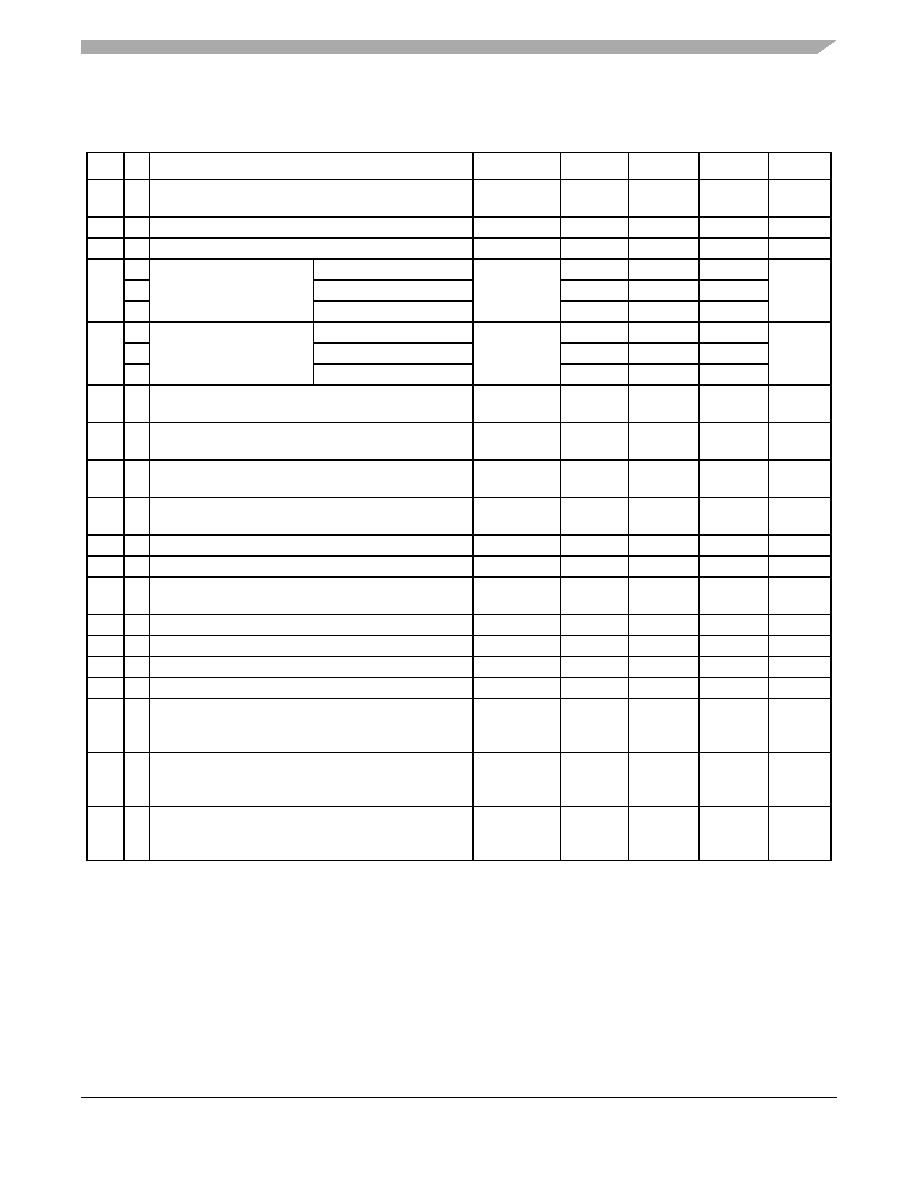
Preliminary Electrical Characteristics
MCF51JM128 ColdFire Microcontroller, Rev. 4
Freescale Semiconductor
27
2.10
MCG Specifications
Table 16. MCG Frequency Specifications (Temperature Range = –40 to 125
C Ambient)
Num C
Rating
Symbol
Min
Typical1
1 Data in Typical column was characterized at 5.0 V, 25C or is typical recommended value
Max
Unit
1P
Internal reference frequency - factory trimmed at VDD
= 5 V and temperature = 25
C
fint_ft
—
32.768
—
kHz
2
P Average internal reference frequency – untrimmed
fint_ut
31.25
—
39.0625
kHz
3
T Internal reference startup time
tirefst
—60
100
s
4
P DCO output frequency
range - untrimmed 2
Low range (DRS=00)
fdco_ut
16
—
20
MHz
P
Mid range (DRS=01)
32
—
40
P
High range (DRS=10)
48
—
60
5
P DCO output frequency2
Reference =32768Hz
and DMX32 = 1
2 The resulting bus clock frequency should not exceed the maximum specified bus clock frequency of the device.
Low range (DRS=00)
fdco_DMX32
—
19.92
—
MHz
P
Mid range (DRS=01)
—
39.85
—
P
High range (DRS=10)
—
59.77
—
6D
Resolution of trimmed DCO output frequency at fixed
voltage and temperature (using FTRIM)
f
dco_res_t
—
0.1
0.2
%fdco
7D
Resolution of trimmed DCO output frequency at fixed
voltage and temperature (not using FTRIM)
f
dco_res_t
—
0.2
0.4
%fdco
8D
Total deviation of trimmed DCO output frequency over
voltage and temperature
f
dco_t
—
0.5
–1.0
2%f
dco
9D
Total deviation of trimmed DCO output frequency over
fixed voltage and temperature range of 0 – 70
C
f
dco_t
—
0.5
1%f
dco
10
D FLL acquisition time 3
3 This specification applies to any time the FLL reference source or reference divider is changed, trim value changed or
changing from FLL disabled (BLPE, BLPI) to FLL enabled (FEI, FEE, FBE, FBI). If a crystal/resonator is being used as the
reference, this specification assumes it is already running.
tfll_acquire
——
1
ms
11
D PLL acquisition time 4
4 This specification applies to any time the PLL VCO divider or reference divider is changed, or changing from PLL disabled
(BLPE, BLPI) to PLL enabled (PBE, PEE). If a crystal/resonator is being used as the reference, this specification assumes
it is already running.
tpll_acquire
——
1
ms
12
D
Long term Jitter of DCO output clock (averaged over
2ms interval) 5
CJitter
—0.02
0.2
%fdco
13
D VCO operating frequency
fvco
7.0
—
55.0
MHz
14
D Jitter of PLL output clock measured over 625 ns6
fpll_jitter_625ns
—0.5665
—%fpll
15
D Lock entry frequency tolerance 7
Dlock
1.49
—
2.98
%
16
D Lock exit frequency tolerance 8
Dunl
4.47
—
5.97
%
17
D Lock time — FLL
tfll_lock
——
tfll_acquire+
1075(1/fint_t
)
s
18
D Lock time — PLL
tpll_lock
——
tpll_acquire+
1075(1/fpll_r
ef)
s
19
D
Loss of external clock minimum frequency – RANGE
= 0
floc_low
(3/5) x fint
—
kHz
相关PDF资料 |
PDF描述 |
|---|---|
| PCF51JM128VQH | MCU 32BIT 128K FLASH 64-QFP |
| PCF51AC256BCLKE | MCU 8BIT 256K FLASH 80-LQFP |
| PCF51AC256BCFUE | MCU 8BIT 256K FLASH 64-QFP |
| PCF51AC256ACPUE | MCU 8BIT 256K FLASH 64-LQFP |
| MK10DN512ZVLK10R | IC ARM CORTEX MCU 512KB 80LQFP |
相关代理商/技术参数 |
参数描述 |
|---|---|
| PCF51JM64VLD | 制造商:Freescale Semiconductor 功能描述:44L 64K FLASH 8K RAM - Trays |
| PCF51JM64VLH | 功能描述:32位微控制器 - MCU RS64L 64K FLASH 8K RAM RoHS:否 制造商:Texas Instruments 核心:C28x 处理器系列:TMS320F28x 数据总线宽度:32 bit 最大时钟频率:90 MHz 程序存储器大小:64 KB 数据 RAM 大小:26 KB 片上 ADC:Yes 工作电源电压:2.97 V to 3.63 V 工作温度范围:- 40 C to + 105 C 封装 / 箱体:LQFP-80 安装风格:SMD/SMT |
| PCF51JM64VLK | 制造商:Freescale Semiconductor 功能描述:RS80L 64K FLASH 8K RAM - Trays |
| PCF51JM64VQH | 制造商:Freescale Semiconductor 功能描述:RS64Q 64K FLASH 8K RAM - Trays |
| PCF51JU128VGM | 制造商:Freescale Semiconductor 功能描述:PCF51JU128VGM - Bulk |
发布紧急采购,3分钟左右您将得到回复。