- 您现在的位置:买卖IC网 > PDF目录3790 > PCF51JM64EVLK (Freescale Semiconductor)MCU 32BIT 64K FLASH 80-LQFP PDF资料下载
参数资料
| 型号: | PCF51JM64EVLK |
| 厂商: | Freescale Semiconductor |
| 文件页数: | 21/49页 |
| 文件大小: | 0K |
| 描述: | MCU 32BIT 64K FLASH 80-LQFP |
| 标准包装: | 90 |
| 系列: | MCF51JM |
| 核心处理器: | Coldfire V1 |
| 芯体尺寸: | 32-位 |
| 速度: | 50MHz |
| 连通性: | CAN,I²C,SCI,SPI,USB OTG |
| 外围设备: | LVD,PWM,WDT |
| 输入/输出数: | 66 |
| 程序存储器容量: | 64KB(64K x 8) |
| 程序存储器类型: | 闪存 |
| RAM 容量: | 16K x 8 |
| 电压 - 电源 (Vcc/Vdd): | 2.7 V ~ 5.5 V |
| 数据转换器: | A/D 12x12b |
| 振荡器型: | 外部 |
| 工作温度: | -40°C ~ 105°C |
| 封装/外壳: | 80-LQFP |
| 包装: | 托盘 |
第1页第2页第3页第4页第5页第6页第7页第8页第9页第10页第11页第12页第13页第14页第15页第16页第17页第18页第19页第20页当前第21页第22页第23页第24页第25页第26页第27页第28页第29页第30页第31页第32页第33页第34页第35页第36页第37页第38页第39页第40页第41页第42页第43页第44页第45页第46页第47页第48页第49页
MCF51JM128 ColdFire Microcontroller, Rev. 4
Preliminary Electrical Characteristics
Freescale Semiconductor
28
2.11
AC Characteristics
This section describes ac timing characteristics for each peripheral system.
2.11.1
Control Timing
5 Jitter is the average deviation from the programmed frequency measured over the specified interval at maximum f
BUS.
Measurements are made with the device powered by filtered supplies and clocked by a stable external clock signal. Noise
injected into the FLL circuitry via VDD and VSS and variation in crystal oscillator frequency increase the CJitter percentage for
a given interval.
6 625 ns represents 5 time quanta for CAN applications, under worst case conditions of 8 MHz CAN bus clock, 1 Mbps CAN
bus speed, and 8 time quanta per bit for bit time settings. 5 time quanta is the minimum time between a synchronization edge
and the sample point of a bit using 8 time quanta per bit.
7 Below D
lock minimum, the MCG is guaranteed to enter lock. Above Dlock maximum, the MCG will not enter lock. But if the
MCG is already in lock, then the MCG may stay in lock.
8 Below D
unl minimum, the MCG will not exit lock if already in lock. Above Dunl maximum, the MCG is guaranteed to exit lock.
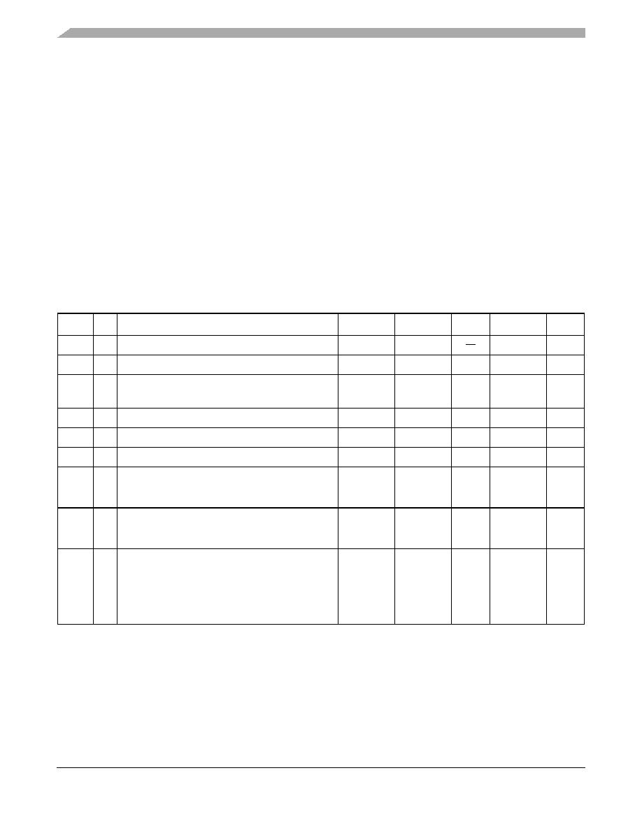
Table 17. Control Timing
Num
C
Parameter
Symbol
Min
Typ1
1 Typical values are based on characterization data at V
DD = 5.0V, 25C unless otherwise stated.
Max
Unit
1
Bus frequency (tcyc = 1/fBus)fBus
dc
—
24
MHz
2
Internal low-power oscillator period
tLPO
700
1300
s
External reset pulse width2
(tcyc = 1/fSelf_reset)
2 This is the shortest pulse guaranteed to be recognized as a reset pin request. Shorter pulses are not guaranteed to override
reset requests from internal sources.
textrst
100
—
ns
4
Reset low drive
trstdrv
66 x tcyc
—ns
5
Active background debug mode latch setup time
tMSSU
500
—
ns
6
Active background debug mode latch hold time
tMSH
100
—
ns
7
IRQ pulse width
Asynchronous path2
Synchronous path3
3 This is the minimum pulse width guaranteed to pass through the pin synchronization circuitry. Shorter pulses may or may not
be recognized. In stop mode, the synchronizer is bypassed so shorter pulses can be recognized in that case.
tILIH, tIHIL
100
1.5 x tcyc
——
ns
8
KBIPx pulse width
Asynchronous path2
Synchronous path3
tILIH, tIHIL
100
1.5 x tcyc
——
ns
9
Port rise and fall time (load = 50 pF)4
Slew rate control disabled (PTxSE = 0) High drive
Slew rate control enabled (PTxSE = 1) High drive
Slew rate control disabled (PTxSE = 0) Low drive
Slew rate control enabled (PTxSE = 1) Low drive
4 Timing is shown with respect to 20% V
DD and 80% VDD levels. Temperature range –40C to 105C.
tRise, tFall
—
11
35
40
75
ns
相关PDF资料 |
PDF描述 |
|---|---|
| PCF51JM128VQH | MCU 32BIT 128K FLASH 64-QFP |
| PCF51AC256BCLKE | MCU 8BIT 256K FLASH 80-LQFP |
| PCF51AC256BCFUE | MCU 8BIT 256K FLASH 64-QFP |
| PCF51AC256ACPUE | MCU 8BIT 256K FLASH 64-LQFP |
| MK10DN512ZVLK10R | IC ARM CORTEX MCU 512KB 80LQFP |
相关代理商/技术参数 |
参数描述 |
|---|---|
| PCF51JM64VLD | 制造商:Freescale Semiconductor 功能描述:44L 64K FLASH 8K RAM - Trays |
| PCF51JM64VLH | 功能描述:32位微控制器 - MCU RS64L 64K FLASH 8K RAM RoHS:否 制造商:Texas Instruments 核心:C28x 处理器系列:TMS320F28x 数据总线宽度:32 bit 最大时钟频率:90 MHz 程序存储器大小:64 KB 数据 RAM 大小:26 KB 片上 ADC:Yes 工作电源电压:2.97 V to 3.63 V 工作温度范围:- 40 C to + 105 C 封装 / 箱体:LQFP-80 安装风格:SMD/SMT |
| PCF51JM64VLK | 制造商:Freescale Semiconductor 功能描述:RS80L 64K FLASH 8K RAM - Trays |
| PCF51JM64VQH | 制造商:Freescale Semiconductor 功能描述:RS64Q 64K FLASH 8K RAM - Trays |
| PCF51JU128VGM | 制造商:Freescale Semiconductor 功能描述:PCF51JU128VGM - Bulk |
发布紧急采购,3分钟左右您将得到回复。