- 您现在的位置:买卖IC网 > PDF目录367933 > PH28F128L18B85 (INTEL CORP) StrataFlash Wireless Memory PDF资料下载
参数资料
| 型号: | PH28F128L18B85 |
| 厂商: | INTEL CORP |
| 元件分类: | PROM |
| 英文描述: | StrataFlash Wireless Memory |
| 中文描述: | 8M X 16 FLASH 1.8V PROM, 85 ns, PBGA56 |
| 封装: | 0.75 MM PITCH, LEAD FREE, VFBGA-56 |
| 文件页数: | 52/106页 |
| 文件大小: | 1272K |
| 代理商: | PH28F128L18B85 |
第1页第2页第3页第4页第5页第6页第7页第8页第9页第10页第11页第12页第13页第14页第15页第16页第17页第18页第19页第20页第21页第22页第23页第24页第25页第26页第27页第28页第29页第30页第31页第32页第33页第34页第35页第36页第37页第38页第39页第40页第41页第42页第43页第44页第45页第46页第47页第48页第49页第50页第51页当前第52页第53页第54页第55页第56页第57页第58页第59页第60页第61页第62页第63页第64页第65页第66页第67页第68页第69页第70页第71页第72页第73页第74页第75页第76页第77页第78页第79页第80页第81页第82页第83页第84页第85页第86页第87页第88页第89页第90页第91页第92页第93页第94页第95页第96页第97页第98页第99页第100页第101页第102页第103页第104页第105页第106页
Intel StrataFlash Wireless Memory (L18)
April 2005
52
Intel StrataFlash Wireless Memory (L18)
Order Number: 251902, Revision: 009
Datasheet
10.3.1
Read Mode
The Read Mode (RM) bit selects synchronous burst-mode or asynchronous page-mode operation
for the device. When the RM bit is set, asynchronous page mode is selected (default). When RM is
cleared, synchronous burst mode is selected.
10.3.2
Latency Count
The Latency Count bits, LC[2:0], tell the device how many clock cycles must elapse from the
rising edge of ADV# (or from the first valid clock edge after ADV# is asserted) until the first data
word is to be driven onto DQ[15:0]. The input clock frequency is used to determine this value.
Figure 24
shows the data output latency for the different settings of LC[2:0].
Synchronous burst with a Latency Count setting of Code 4 will result in zero WAIT state; however,
a Latency Count setting of Code 5 will cause 1 WAIT state (Code 6 will cause 2 WAIT states, and
Code 7 will cause 3 WAIT states) after every four words, regardless of whether a 16-word
boundary is crossed. If RCR[9] (Data Hold) bit is set (data hold of two clocks) this WAIT condition
will not occur because enough clocks elapse during each burst cycle to eliminate subsequent WAIT
states.
Refer to
Table 11
and
Table 12
for Latency Code Settings.
15
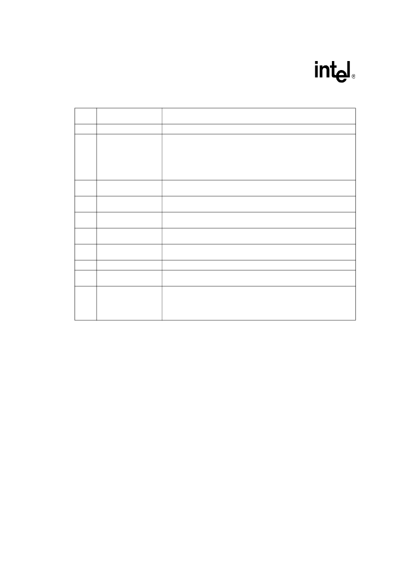
Read Mode (RM)
0 = Synchronous burst-mode read
1 = Asynchronous page-mode read (default)
14
Reserved (R)
Reserved bits should be cleared (0)
13:11
Latency Count (LC[2:0])
010 =Code 2
011 =Code 3
100 =Code 4
101 =Code 5
110 =Code 6
111 =Code 7 (default)
(Other bit settings are reserved)
10
Wait Polarity (WP)
0 =WAIT signal is active low
1 =WAIT signal is active high (default)
9
Data Hold (DH)
0 =Data held for a 1-clock data cycle
1 =Data held for a 2-clock data cycle (default)
8
Wait Delay (WD)
0 =WAIT deasserted with valid data
1 =WAIT deasserted one data cycle before valid data (default)
7
Burst Sequence (BS)
0 =Reserved
1 =Linear (default)
6
Clock Edge (CE)
0 = Falling edge
1 = Rising edge (default)
5:4
Reserved (R)
Reserved bits should be cleared (0)
3
Burst Wrap (BW)
0 =Wrap; Burst accesses wrap within burst length set by BL[2:0]
1 =No Wrap; Burst accesses do not wrap within burst length (default)
2:0
Burst Length (BL[2:0])
001 =4-word burst
010 =8-word burst
011 =16-word burst
111 =Continuous-word burst (default)
(Other bit settings are reserved)
Note:
Latency Code 2, Data Hold for a 2-clock data cycle (DH = 1)
Wait must be deasserted with valid data (WD =
0). WD = 1 is not supported.
Table 10.
Read Configuration Register Description (Sheet 2 of 2)
相关PDF资料 |
PDF描述 |
|---|---|
| PH28F128L18T85 | StrataFlash Wireless Memory |
| PH28F256L18B85 | StrataFlash Wireless Memory |
| PH28F256L18T85 | StrataFlash Wireless Memory |
| PH28F640L18B85 | StrataFlash Wireless Memory |
| PH28F640L18T85 | StrataFlash Wireless Memory |
相关代理商/技术参数 |
参数描述 |
|---|---|
| PH28F128L18B85A | 制造商:Micron Technology Inc 功能描述:128MB, TYAX .75 VFBGA 1.8 LF - Trays |
| PH28F128L18T85 | 制造商:INTEL 制造商全称:Intel Corporation 功能描述:StrataFlash Wireless Memory |
| PH28F128W18BD60A | 制造商:Micron Technology Inc 功能描述:NOR Flash Parallel 1.8V 128Mbit 8M x 16bit 60ns 56-Pin VFBGA Tray |
| PH28F160C3BD70A | 制造商:Micron Technology Inc 功能描述:MM#865392FLASH 28F160C3BD 70 VF-PBGA46 C |
| PH28F256L18B85 | 制造商:INTEL 制造商全称:Intel Corporation 功能描述:StrataFlash Wireless Memory |
发布紧急采购,3分钟左右您将得到回复。