- 您现在的位置:买卖IC网 > PDF目录96680 > PI5A751AT (PERICOM SEMICONDUCTOR CORP) 2-CHANNEL, AUDIO/VIDEO SWITCH, PDSO6 PDF资料下载
参数资料
| 型号: | PI5A751AT |
| 厂商: | PERICOM SEMICONDUCTOR CORP |
| 元件分类: | 多路复用及模拟开关 |
| 英文描述: | 2-CHANNEL, AUDIO/VIDEO SWITCH, PDSO6 |
| 封装: | SOT-23, 6 PIN |
| 文件页数: | 2/8页 |
| 文件大小: | 343K |
| 代理商: | PI5A751AT |
2
PXXXX
03/06/01
12345678901234567890123456789012123456789012345678901234567890121234567890123456789012345678901212345678901234567890123456789012123456789012
ADVANCE INFORMATION
PI5A571A
CMOS Low Voltage RF/Video, SPST Switch
VDD to GND............................................................. 0.3 V to +6 V
Analog, Digital Inputs(2) .......................... 0.3 V to VDD +0.3 V or
30mA, Whichever Occurs First
Peak Current, S or D ...........................................................100mA
(Pulsed at 1ms, 10% Duty Cycle Max)
Continuous Current, S or D ................................................ 30 mA
Operating Temperature Range
Industrial (A, B Versions ...................................... 40°C to +85°C
Storage Temperature Range ............................... 65°C to +150°C
Junction Temperature (TJ Max)......................................... +150°C
ElectricalSpecifications
(VDD = 5V ±10%, GND = 0V, unless otherwise noted.
r
e
t
e
m
a
r
a
Pl
o
b
m
y
Ss
n
o
it
i
d
n
o
C.
p
m
e
T.
n
i
M.
p
y
T.
x
a
Ms
ti
n
U
h
c
ti
w
S
g
o
l
a
n
A
e
g
n
a
R
l
a
n
g
i
S
g
o
l
a
n
A
.
p
m
e
T0
V D
D
V
e
c
n
a
t
si
s
e
R
n
OR N
O
VS
V
o
t
V
0
=
D
I
, S
D
.
1
ti
u
c
ri
c
t
s
e
t
e
s
,
A
m
0
1
=
5
25
18
1
.
p
m
e
T0
2
s
e
n
t
al
F
e
c
n
a
t
si
s
e
R
-
n
O
R T
A
L
F
)
N
O
(
VS
I
,
V
5
.
2
o
t
V
0
=
S
D
V
,
A
m
0
1
=
D
V
5
.
4
=.
p
m
e
T3
t
n
e
r
u
C
e
g
a
k
a
e
L
ff
O
SI
)
F
O
(
S
VS
V
,
V
1
/
V
5
.
4
=
S
.
2
ti
u
c
ri
c
t
s
e
t
e
s
,
V
5
.
4
/
V
1
=
5
21
0
.
05
2
.
0
A
n
.
p
m
e
T3
t
n
e
r
u
C
e
g
a
k
a
e
L
ff
O
DI
)
F
O
(
D
VS
V
,
V
1
/
V
5
.
4
=
S
.
2
ti
u
c
ri
c
t
s
e
t
e
s
,
V
5
.
4
/
V
1
=
5
25
2
.
0
A
n
.
p
m
e
T3
l
e
n
a
h
C
n
O
D
,
S
e
g
a
k
a
e
L
I M
O
C
)
N
O
(
VD V
= S
.
3
ti
u
c
ri
c
t
s
e
t
e
s
,
V
5
.
4
r
o
V
1
=
5
21
0
.
0
A
n
.
p
m
e
T5
2
.
03
s
t
u
p
n
I
l
a
ti
g
i
D
e
g
a
tl
o
V
h
g
i
H
t
u
p
n
IV H
I
.
p
m
e
T4
.
2V
e
g
a
tl
o
V
w
o
L
t
u
p
n
IV H
I
.
p
m
e
T8
.
0V
t
n
e
r
u
C
t
u
p
n
II H
I
, L
I
.
p
m
e
T5
.
0A
e
c
n
a
ti
c
a
p
a
C
t
u
p
n
I
l
a
ti
g
i
DC N
I
5
22
F
p
s
c
it
s
i
r
e
t
c
a
r
a
h
C
g
n
i
h
c
ti
w
S
d
n
a
c
i
m
a
n
y
D
e
m
i
T
g
n
i
h
c
ti
w
S
n
Ot N
O
V
,
4
ti
u
c
ri
C
t
s
e
T
S
R
,
V
3
=
L
0
3
=
C
, L
F
p
5
3
=
5
29
s
n
.
p
m
e
T3
1
e
m
i
T
g
n
i
h
c
ti
w
S
ff
Ot F
F
O
V
,
4
ti
u
c
ri
C
t
s
e
T
S
R
,
V
3
=
L
0
3
=
C
, L
F
p
5
3
=
5
23
s
n
.
p
m
e
T5
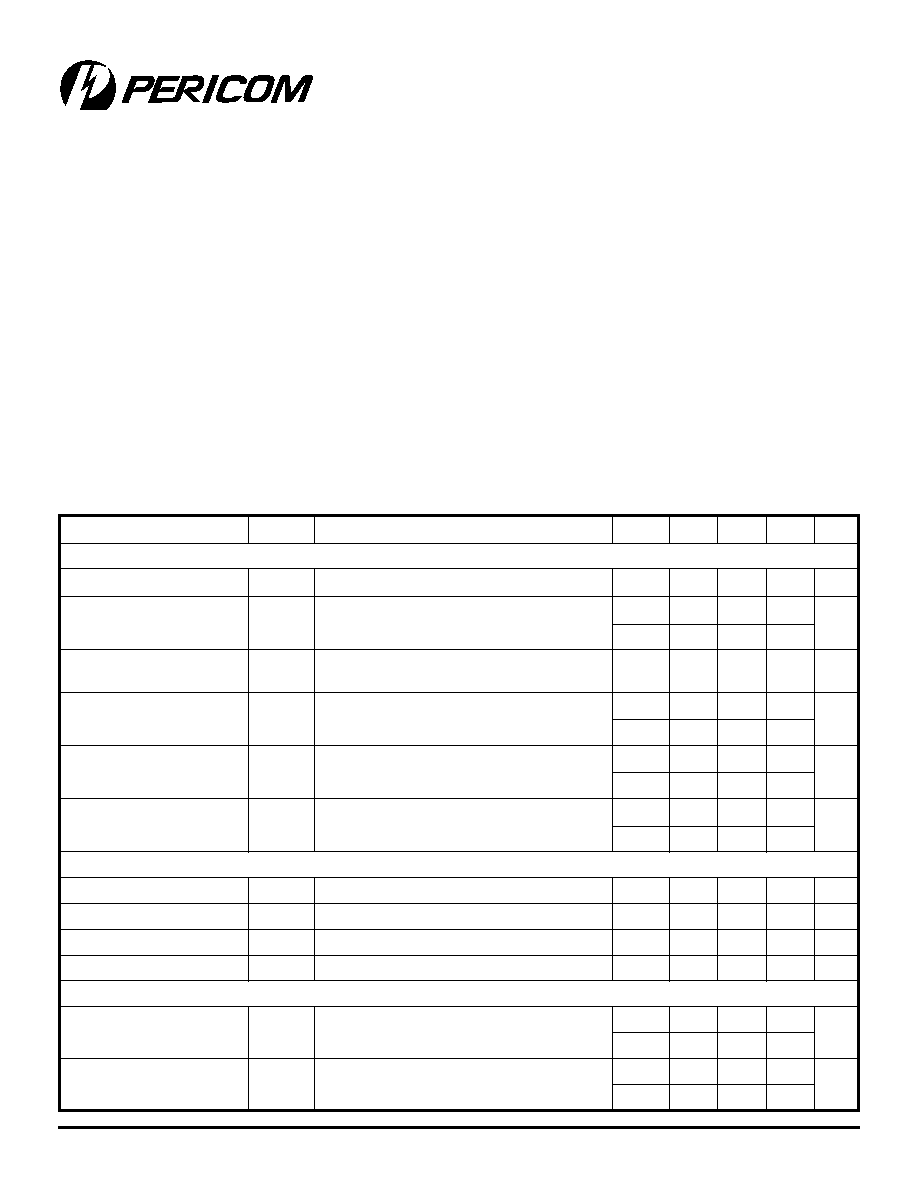
Absolute Maximum Ratings (TA = +25°C unless otherwise noted)
Power Dissipation .............................................. (TJ MaxTA)/θJA
MSOP Package
θJA Thermal Impedance................................................... 206°C/W
θJC Thermal Impedance .................................................... 44°C/W
SOT Package
θJA Thermal Impedance................................................ 229.6°C/W
θJC Thermal Impedance .............................................. 91.99°C/W
Lead Temperature, Soldering
Vapor Phase (60s) .............................................................. +215°C
Infrared (15s) ..................................................................... +220°C
Notes:
1. Stresses above those listed under Absolute Maximum Ratings may cause permanent damage to the device. This is a stress rating
only; functional operation of the device at these or any other conditions above those listed in the operational sections of this
specification is not implied. Exposure to absolute maximum rating conditions for extended periods may affect device reliability. Only
one absolute maximum rating may be applied at any one time.
2. Overvoltages at IN, S or D will be clamped by internal diodes. Current should be limited to the maximum ratings given.
相关PDF资料 |
PDF描述 |
|---|---|
| PI5A751AU | 2-CHANNEL, AUDIO/VIDEO SWITCH, PDSO8 |
| PI5V330QEX | QUAD 2-CHANNEL, VIDEO MULTIPLEXER, PDSO16 |
| PI5V330SE | QUAD 2-CHANNEL, VIDEO MULTIPLEXER, PDSO16 |
| PI5V330SW | QUAD 2-CHANNEL, VIDEO MULTIPLEXER, PDSO16 |
| PI5V330SX | QUAD 2-CHANNEL, VIDEO MULTIPLEXER, PDSO16 |
相关代理商/技术参数 |
参数描述 |
|---|---|
| PI5C16209 | 制造商:未知厂家 制造商全称:未知厂家 功能描述:Digital Switch | 18-Bit Bus Exchange Switch |
| PI5C16209A | 制造商:未知厂家 制造商全称:未知厂家 功能描述:Bus Exchanger |
| PI5C16209V | 制造商:未知厂家 制造商全称:未知厂家 功能描述:Bus Exchanger |
| PI5C16210 | 制造商:PERICOM 制造商全称:Pericom Semiconductor Corporation 功能描述:20-Bit, 2-Port Bus Switch |
| PI5C16210A | 制造商:PERICOM 制造商全称:Pericom Semiconductor Corporation 功能描述:BUS SWITCH|CMOS|TSSOP|48PIN|PLASTIC |
发布紧急采购,3分钟左右您将得到回复。