- 您现在的位置:买卖IC网 > PDF目录11527 > PIC12C671-10E/P (Microchip Technology)IC MCU OTP 1KX14 A/D 8DIP PDF资料下载
参数资料
| 型号: | PIC12C671-10E/P |
| 厂商: | Microchip Technology |
| 文件页数: | 77/129页 |
| 文件大小: | 0K |
| 描述: | IC MCU OTP 1KX14 A/D 8DIP |
| 产品培训模块: | Asynchronous Stimulus |
| 标准包装: | 60 |
| 系列: | PIC® 12C |
| 核心处理器: | PIC |
| 芯体尺寸: | 8-位 |
| 速度: | 10MHz |
| 外围设备: | POR,WDT |
| 输入/输出数: | 5 |
| 程序存储器容量: | 1.75KB(1K x 14) |
| 程序存储器类型: | OTP |
| RAM 容量: | 128 x 8 |
| 电压 - 电源 (Vcc/Vdd): | 3 V ~ 5.5 V |
| 数据转换器: | A/D 4x8b |
| 振荡器型: | 内部 |
| 工作温度: | -40°C ~ 125°C |
| 封装/外壳: | 8-DIP(0.300",7.62mm) |
| 包装: | 管件 |
第1页第2页第3页第4页第5页第6页第7页第8页第9页第10页第11页第12页第13页第14页第15页第16页第17页第18页第19页第20页第21页第22页第23页第24页第25页第26页第27页第28页第29页第30页第31页第32页第33页第34页第35页第36页第37页第38页第39页第40页第41页第42页第43页第44页第45页第46页第47页第48页第49页第50页第51页第52页第53页第54页第55页第56页第57页第58页第59页第60页第61页第62页第63页第64页第65页第66页第67页第68页第69页第70页第71页第72页第73页第74页第75页第76页当前第77页第78页第79页第80页第81页第82页第83页第84页第85页第86页第87页第88页第89页第90页第91页第92页第93页第94页第95页第96页第97页第98页第99页第100页第101页第102页第103页第104页第105页第106页第107页第108页第109页第110页第111页第112页第113页第114页第115页第116页第117页第118页第119页第120页第121页第122页第123页第124页第125页第126页第127页第128页第129页
1999 Microchip Technology Inc.
DS30561B-page 51
PIC12C67X
8.5
A/D Operation During Sleep
The A/D module can operate during SLEEP mode. This
requires that the A/D clock source be set to RC
(ADCS<1:0> = 11). When the RC clock source is
selected, the A/D module waits one instruction cycle
before starting the conversion. This allows the SLEEP
instruction to be executed, which eliminates all digital
switching noise from the conversion. When the conver-
sion is completed, the GO/DONE bit will be cleared,
and the result loaded into the ADRES Register. If the
A/D interrupt is enabled, the device will wake-up from
SLEEP. If the A/D interrupt is not enabled, the A/D mod-
ule will then be turned off, although the ADON bit will
remain set.
When the A/D clock source is another clock option (not
RC), a SLEEP instruction will cause the present conver-
sion to be aborted and the A/D module to be turned off,
though the ADON bit will remain set.
Turning off the A/D places the A/D module in its lowest
current consumption state.
8.6
A/D Accuracy/Error
The overall accuracy of the A/D is less than
± 1 LSb for
VDD = 5V
± 10% and the analog VREF = VDD. This over-
all accuracy includes offset error, full scale error, and
integral error. The A/D converter is monotonic over the
full VDD range. The resolution and accuracy may be
less when either the analog reference (VDD) is less than
5.0V or when the analog reference (VREF) is less than
VDD.
The maximum pin leakage current is specified in the
Device Data Sheet electrical specification, parameter
#D060.
In systems where the device frequency is low, use of
the A/D RC clock is preferred. At moderate to high fre-
quencies, TAD should be derived from the device oscil-
lator. TAD must not violate the minimum and should be
≤8 s for preferred operation. This is because TAD,
when derived from TOSC, is kept away from on-chip
phase clock transitions. This reduces, to a large extent,
the effects of digital switching noise. This is not possible
with the RC derived clock. The loss of accuracy due to
digital switching noise can be significant if many I/O
pins are active.
In systems where the device will enter SLEEP mode
after the start of the A/D conversion, the RC clock
source selection is required. In this mode, the digital
noise from the modules in SLEEP are stopped. This
method gives high accuracy.
Note:
For the A/D module to operate in SLEEP,
the A/D clock source must be set to RC
(ADCS<1:0> = 11). To perform an A/D
conversion in SLEEP, the GO/DONE bit
must be set, followed by the SLEEP
instruction.
8.7
Effects of a Reset
A device reset forces all registers to their reset state.
This forces the A/D module to be turned off, and any
conversion is aborted. The value that is in the ADRES
register is not modified for a Reset. The ADRES regis-
ter will contain unknown data after a Power-on Reset.
8.8
Connection Considerations
If the input voltage exceeds the rail values (VSS or VDD)
by greater than 0.2V, then the accuracy of the conver-
sion is out of specification.
An external RC filter is sometimes added for anti-
aliasing of the input signal. The R component should be
selected to ensure that the total source impedance is
kept under the 10 k
recommended specification. Any
external components connected (via hi-impedance) to
an analog input pin (capacitor, zener diode, etc.) should
have very little leakage current at the pin.
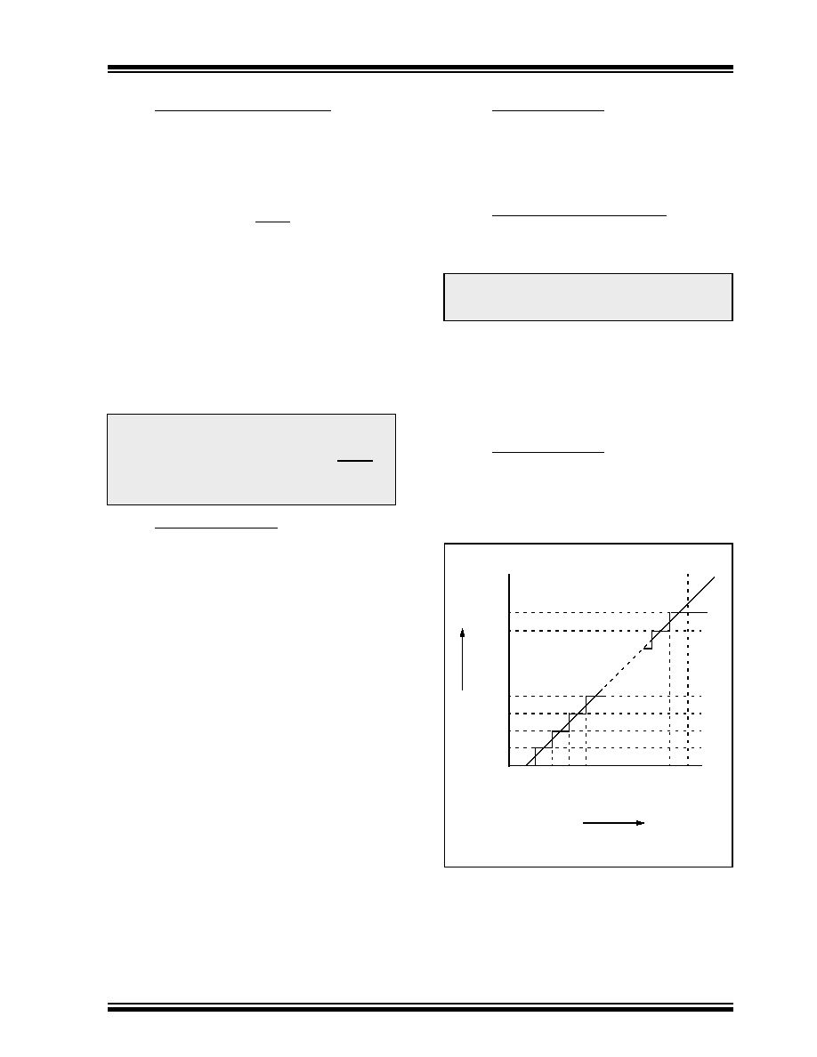
8.9
Transfer Function
The ideal transfer function of the A/D converter is as fol-
lows: the first transition occurs when the analog input
voltage (VAIN) is 1 LSb (or Analog VREF / 256)
FIGURE 8-3:
A/D TRANSFER FUNCTION
Note:
For the PIC12C67X, care must be taken
when using the GP4 pin in A/D conversions
due to its proximity to the OSC1 pin.
Digit
al
code
out
put
FFh
FEh
04h
03h
02h
01h
00h
0.
5
LS
b
1
LSb
2
LSb
3
LSb
4
LSb
255
LS
b
256
LS
b
(f
ull
sc
al
e)
Analog input voltage
相关PDF资料 |
PDF描述 |
|---|---|
| PIC16LC57C-04/SO | IC MCU OTP 2KX12 28SOIC |
| VI-27M-IY-B1 | CONVERTER MOD DC/DC 10V 50W |
| VI-27L-IY-B1 | CONVERTER MOD DC/DC 28V 50W |
| PIC24F16KA101-E/SO | MCU 16KB FLASH 1.5KB RAM 20SOIC |
| PIC16CE623-04/SS | IC MCU OTP 512X14 EE COMP 20SSOP |
相关代理商/技术参数 |
参数描述 |
|---|---|
| PIC12C671-10I | 制造商:MICROCHIP 制造商全称:Microchip Technology 功能描述:8-Pin, 8-Bit CMOS Microcontroller with A/D Converter |
| PIC12C671-10I/JM | 制造商:MICROCHIP 制造商全称:Microchip Technology 功能描述:8-Pin, 8-Bit CMOS Microcontroller with A/D Converter |
| PIC12C671-10I/JW | 制造商:未知厂家 制造商全称:未知厂家 功能描述:MICROCONTROLLER|8-BIT|PIC CPU|CMOS|DIP|8PIN|CERAMIC |
| PIC12C671-10I/MF | 功能描述:8位微控制器 -MCU 1.75KB 128 RAM 6 I/O 10MHz IndTemp DFN8 RoHS:否 制造商:Silicon Labs 核心:8051 处理器系列:C8051F39x 数据总线宽度:8 bit 最大时钟频率:50 MHz 程序存储器大小:16 KB 数据 RAM 大小:1 KB 片上 ADC:Yes 工作电源电压:1.8 V to 3.6 V 工作温度范围:- 40 C to + 105 C 封装 / 箱体:QFN-20 安装风格:SMD/SMT |
| PIC12C671-10I/P | 功能描述:8位微控制器 -MCU 1.75KB 128 RAM 6 I/O 10MHz IndTemp PDIP8 RoHS:否 制造商:Silicon Labs 核心:8051 处理器系列:C8051F39x 数据总线宽度:8 bit 最大时钟频率:50 MHz 程序存储器大小:16 KB 数据 RAM 大小:1 KB 片上 ADC:Yes 工作电源电压:1.8 V to 3.6 V 工作温度范围:- 40 C to + 105 C 封装 / 箱体:QFN-20 安装风格:SMD/SMT |
发布紧急采购,3分钟左右您将得到回复。