- 您现在的位置:买卖IC网 > PDF目录1962 > PIC12HV752-E/P (Microchip Technology)IC MCU 8BIT 1024B FLASH 8-PDIP PDF资料下载
参数资料
| 型号: | PIC12HV752-E/P |
| 厂商: | Microchip Technology |
| 文件页数: | 124/201页 |
| 文件大小: | 0K |
| 描述: | IC MCU 8BIT 1024B FLASH 8-PDIP |
| 标准包装: | 60 |
| 系列: | PIC® 12F |
| 核心处理器: | PIC |
| 芯体尺寸: | 8-位 |
| 速度: | 20MHz |
| 外围设备: | 欠压检测/复位,POR,PWM,WDT |
| 输入/输出数: | 5 |
| 程序存储器容量: | 1.75KB(1K x 14) |
| 程序存储器类型: | 闪存 |
| RAM 容量: | 64 x 8 |
| 电压 - 电源 (Vcc/Vdd): | 2 V ~ 5 V |
| 数据转换器: | A/D 4x10b |
| 振荡器型: | 内部 |
| 工作温度: | -40°C ~ 125°C |
| 封装/外壳: | 8-DIP(0.300",7.62mm) |
| 包装: | 管件 |
第1页第2页第3页第4页第5页第6页第7页第8页第9页第10页第11页第12页第13页第14页第15页第16页第17页第18页第19页第20页第21页第22页第23页第24页第25页第26页第27页第28页第29页第30页第31页第32页第33页第34页第35页第36页第37页第38页第39页第40页第41页第42页第43页第44页第45页第46页第47页第48页第49页第50页第51页第52页第53页第54页第55页第56页第57页第58页第59页第60页第61页第62页第63页第64页第65页第66页第67页第68页第69页第70页第71页第72页第73页第74页第75页第76页第77页第78页第79页第80页第81页第82页第83页第84页第85页第86页第87页第88页第89页第90页第91页第92页第93页第94页第95页第96页第97页第98页第99页第100页第101页第102页第103页第104页第105页第106页第107页第108页第109页第110页第111页第112页第113页第114页第115页第116页第117页第118页第119页第120页第121页第122页第123页当前第124页第125页第126页第127页第128页第129页第130页第131页第132页第133页第134页第135页第136页第137页第138页第139页第140页第141页第142页第143页第144页第145页第146页第147页第148页第149页第150页第151页第152页第153页第154页第155页第156页第157页第158页第159页第160页第161页第162页第163页第164页第165页第166页第167页第168页第169页第170页第171页第172页第173页第174页第175页第176页第177页第178页第179页第180页第181页第182页第183页第184页第185页第186页第187页第188页第189页第190页第191页第192页第193页第194页第195页第196页第197页第198页第199页第200页第201页
29
7682C–AUTO–04/08
AT90CAN32/64/128
4.5.3
Address Latch Requirements
Due to the high-speed operation of the XRAM interface, the address latch must be selected with
care for system frequencies above 8 MHz @ 4V and 4 MHz @ 2.7V. When operating at condi-
tions above these frequencies, the typical old style 74HC series latch becomes inadequate. The
External Memory Interface is designed in compliance to the 74AHC series latch. However, most
latches can be used as long they comply with the main timing parameters. The main parameters
for the address latch are:
D to Q propagation delay (tPD).
Data setup time before G low (tSU).
Data (address) hold time after G low (TH).
The External Memory Interface is designed to guaranty minimum address hold time after G is
asserted low of th = 5 ns. Refer to tLAXX_LD / tLLAXX_ST in “Memory Programming” Tables 26-7
through Tables 26-14. The D-to-Q propagation delay (tPD) must be taken into consideration
when calculating the access time requirement of the external component. The data setup time
before G low (tSU) must not exceed address valid to ALE low (tAVLLC) minus PCB wiring delay
(dependent on the capacitive load).
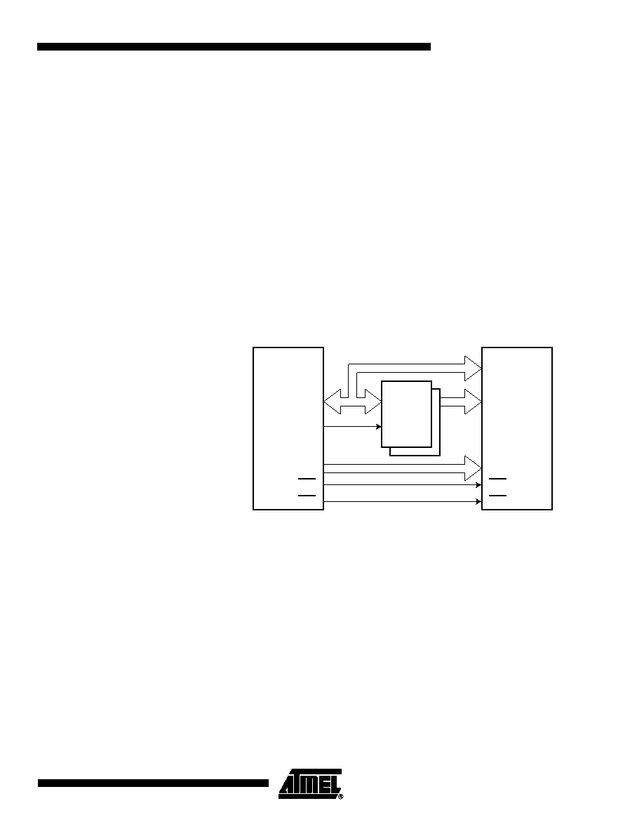
Figure 4-5.
External SRAM Connected to the AVR
4.5.4
Pull-up and Bus-keeper
The pull-ups on the AD7:0 ports may be activated if the corresponding Port register is written to
one. To reduce power consumption in sleep mode, it is recommended to disable the pull-ups by
writing the Port register to zero before entering sleep.
The XMEM interface also provides a bus-keeper on the AD7:0 lines. The bus-keeper can be dis-
abled and enabled in software as described in “External Memory Control Register B – XMCRB”
on page 33. When enabled, the bus-keeper will ensure a defined logic level (zero or one) on the
AD7:0 bus when these lines would otherwise be tri-stated by the XMEM interface.
4.5.5
Timing
External Memory devices have different timing requirements. To meet these requirements, the
AT90CAN32/64/128 XMEM interface provides four different wait-states as shown in Table 4-4. It
is important to consider the timing specification of the External Memory device before selecting
the wait-state. The most important parameters are the access time for the external memory
compared to the set-up requirement of the AT90CAN32/64/128. The access time for the Exter-
nal Memory is defined to be the time from receiving the chip select/address until the data of this
D[7:0]
A[7:0]
A[15:8]
RD
WR
SRAM
D
Q
G
AD7:0
ALE
A15:8
RD
WR
AVR
相关PDF资料 |
PDF描述 |
|---|---|
| PIC12LF1501-E/MC | IC MCU 8BIT 1.75KB FLASH 8DFN |
| PIC12LF1501-I/MF | IC MCU 8BIT 1.75KB FLASH 8-DFN |
| PIC14000-04I/SO | IC MCU OTP 4KX14 A/D 28SOIC |
| PIC16C432T-I/SS | IC MCU CMOS 8BIT 20MHZ 2K 20SSOP |
| PIC16C433-I/SO | IC MCU CMOS 8BIT 10MHZ 2K 18SOIC |
相关代理商/技术参数 |
参数描述 |
|---|---|
| PIC12HV752-I/MF | 功能描述:8位微控制器 -MCU 1.75KB 64BRAM 6 I/O 8MHz Int Osc 5MIPS RoHS:否 制造商:Silicon Labs 核心:8051 处理器系列:C8051F39x 数据总线宽度:8 bit 最大时钟频率:50 MHz 程序存储器大小:16 KB 数据 RAM 大小:1 KB 片上 ADC:Yes 工作电源电压:1.8 V to 3.6 V 工作温度范围:- 40 C to + 105 C 封装 / 箱体:QFN-20 安装风格:SMD/SMT |
| PIC12HV752-I/P | 功能描述:8位微控制器 -MCU 1.75KB 64BRAM 6 I/O 8MHz Int Osc 5MIPS RoHS:否 制造商:Silicon Labs 核心:8051 处理器系列:C8051F39x 数据总线宽度:8 bit 最大时钟频率:50 MHz 程序存储器大小:16 KB 数据 RAM 大小:1 KB 片上 ADC:Yes 工作电源电压:1.8 V to 3.6 V 工作温度范围:- 40 C to + 105 C 封装 / 箱体:QFN-20 安装风格:SMD/SMT |
| PIC12HV752-I/SN | 功能描述:8位微控制器 -MCU 1.75KB 64BRAM 6 I/O 8MHz Int Osc 5MIPS RoHS:否 制造商:Silicon Labs 核心:8051 处理器系列:C8051F39x 数据总线宽度:8 bit 最大时钟频率:50 MHz 程序存储器大小:16 KB 数据 RAM 大小:1 KB 片上 ADC:Yes 工作电源电压:1.8 V to 3.6 V 工作温度范围:- 40 C to + 105 C 封装 / 箱体:QFN-20 安装风格:SMD/SMT |
| PIC12HV752T-I/MF | 功能描述:8位微控制器 -MCU 1.75KB 64BRAM 6 I/O 8MHz Int Osc 5MIPS RoHS:否 制造商:Silicon Labs 核心:8051 处理器系列:C8051F39x 数据总线宽度:8 bit 最大时钟频率:50 MHz 程序存储器大小:16 KB 数据 RAM 大小:1 KB 片上 ADC:Yes 工作电源电压:1.8 V to 3.6 V 工作温度范围:- 40 C to + 105 C 封装 / 箱体:QFN-20 安装风格:SMD/SMT |
| PIC12HV752T-I/SN | 功能描述:8位微控制器 -MCU 1.75KB 64BRAM 6 I/O 8MHz Int Osc 5MIPS RoHS:否 制造商:Silicon Labs 核心:8051 处理器系列:C8051F39x 数据总线宽度:8 bit 最大时钟频率:50 MHz 程序存储器大小:16 KB 数据 RAM 大小:1 KB 片上 ADC:Yes 工作电源电压:1.8 V to 3.6 V 工作温度范围:- 40 C to + 105 C 封装 / 箱体:QFN-20 安装风格:SMD/SMT |
发布紧急采购,3分钟左右您将得到回复。