- 您现在的位置:买卖IC网 > PDF目录1962 > PIC12HV752-E/P (Microchip Technology)IC MCU 8BIT 1024B FLASH 8-PDIP PDF资料下载
参数资料
| 型号: | PIC12HV752-E/P |
| 厂商: | Microchip Technology |
| 文件页数: | 77/201页 |
| 文件大小: | 0K |
| 描述: | IC MCU 8BIT 1024B FLASH 8-PDIP |
| 标准包装: | 60 |
| 系列: | PIC® 12F |
| 核心处理器: | PIC |
| 芯体尺寸: | 8-位 |
| 速度: | 20MHz |
| 外围设备: | 欠压检测/复位,POR,PWM,WDT |
| 输入/输出数: | 5 |
| 程序存储器容量: | 1.75KB(1K x 14) |
| 程序存储器类型: | 闪存 |
| RAM 容量: | 64 x 8 |
| 电压 - 电源 (Vcc/Vdd): | 2 V ~ 5 V |
| 数据转换器: | A/D 4x10b |
| 振荡器型: | 内部 |
| 工作温度: | -40°C ~ 125°C |
| 封装/外壳: | 8-DIP(0.300",7.62mm) |
| 包装: | 管件 |
第1页第2页第3页第4页第5页第6页第7页第8页第9页第10页第11页第12页第13页第14页第15页第16页第17页第18页第19页第20页第21页第22页第23页第24页第25页第26页第27页第28页第29页第30页第31页第32页第33页第34页第35页第36页第37页第38页第39页第40页第41页第42页第43页第44页第45页第46页第47页第48页第49页第50页第51页第52页第53页第54页第55页第56页第57页第58页第59页第60页第61页第62页第63页第64页第65页第66页第67页第68页第69页第70页第71页第72页第73页第74页第75页第76页当前第77页第78页第79页第80页第81页第82页第83页第84页第85页第86页第87页第88页第89页第90页第91页第92页第93页第94页第95页第96页第97页第98页第99页第100页第101页第102页第103页第104页第105页第106页第107页第108页第109页第110页第111页第112页第113页第114页第115页第116页第117页第118页第119页第120页第121页第122页第123页第124页第125页第126页第127页第128页第129页第130页第131页第132页第133页第134页第135页第136页第137页第138页第139页第140页第141页第142页第143页第144页第145页第146页第147页第148页第149页第150页第151页第152页第153页第154页第155页第156页第157页第158页第159页第160页第161页第162页第163页第164页第165页第166页第167页第168页第169页第170页第171页第172页第173页第174页第175页第176页第177页第178页第179页第180页第181页第182页第183页第184页第185页第186页第187页第188页第189页第190页第191页第192页第193页第194页第195页第196页第197页第198页第199页第200页第201页
168
7682C–AUTO–04/08
AT90CAN32/64/128
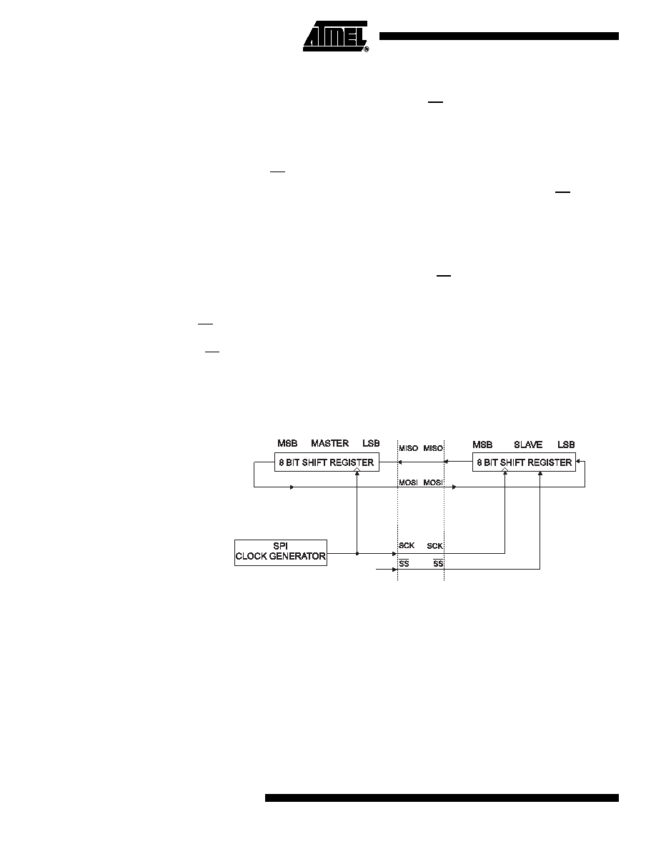
The interconnection between Master and Slave CPUs with SPI is shown in Figure 16-2. The sys-
tem consists of two shift Registers, and a Master clock generator. The SPI Master initiates the
communication cycle when pulling low the Slave Select SS pin of the desired Slave. Master and
Slave prepare the data to be sent in their respective shift Registers, and the Master generates
the required clock pulses on the SCK line to interchange data. Data is always shifted from Mas-
ter to Slave on the Master Out – Slave In, MOSI, line, and from Slave to Master on the Master In
– Slave Out, MISO, line. After each data packet, the Master will synchronize the Slave by pulling
high the Slave Select, SS, line.
When configured as a Master, the SPI interface has no automatic control of the SS line. This
must be handled by user software before communication can start. When this is done, writing a
byte to the SPI Data Register starts the SPI clock generator, and the hardware shifts the eight
bits into the Slave. After shifting one byte, the SPI clock generator stops, setting the end of
transmission flag (SPIF). If the SPI Interrupt Enable bit (SPIE) in the SPCR Register is set, an
interrupt is requested. The Master may continue to shift the next byte by writing it into SPDR, or
signal the end of packet by pulling high the Slave Select, SS line. The last incoming byte will be
kept in the Buffer Register for later use.
When configured as a Slave, the SPI interface will remain sleeping with MISO tri-stated as long
as the SS pin is driven high. In this state, software may update the contents of the SPI Data
Register, SPDR, but the data will not be shifted out by incoming clock pulses on the SCK pin
until the SS pin is driven low. As one byte has been completely shifted, the end of transmission
flag, SPIF is set. If the SPI Interrupt Enable bit, SPIE, in the SPCR Register is set, an interrupt is
requested. The Slave may continue to place new data to be sent into SPDR before reading the
incoming data. The last incoming byte will be kept in the Buffer Register for later use.
Figure 16-2. SPI Master-slave Interconnection
The system is single buffered in the transmit direction and double buffered in the receive direc-
tion. This means that bytes to be transmitted cannot be written to the SPI Data Register before
the entire shift cycle is completed. When receiving data, however, a received character must be
read from the SPI Data Register before the next character has been completely shifted in. Oth-
erwise, the first byte is lost.
In SPI Slave mode, the control logic will sample the incoming signal of the SCK pin. To ensure
correct sampling of the clock signal, the frequency of the SPI clock should never exceed fclkio/4.
SHIFT
ENABLE
相关PDF资料 |
PDF描述 |
|---|---|
| PIC12LF1501-E/MC | IC MCU 8BIT 1.75KB FLASH 8DFN |
| PIC12LF1501-I/MF | IC MCU 8BIT 1.75KB FLASH 8-DFN |
| PIC14000-04I/SO | IC MCU OTP 4KX14 A/D 28SOIC |
| PIC16C432T-I/SS | IC MCU CMOS 8BIT 20MHZ 2K 20SSOP |
| PIC16C433-I/SO | IC MCU CMOS 8BIT 10MHZ 2K 18SOIC |
相关代理商/技术参数 |
参数描述 |
|---|---|
| PIC12HV752-I/MF | 功能描述:8位微控制器 -MCU 1.75KB 64BRAM 6 I/O 8MHz Int Osc 5MIPS RoHS:否 制造商:Silicon Labs 核心:8051 处理器系列:C8051F39x 数据总线宽度:8 bit 最大时钟频率:50 MHz 程序存储器大小:16 KB 数据 RAM 大小:1 KB 片上 ADC:Yes 工作电源电压:1.8 V to 3.6 V 工作温度范围:- 40 C to + 105 C 封装 / 箱体:QFN-20 安装风格:SMD/SMT |
| PIC12HV752-I/P | 功能描述:8位微控制器 -MCU 1.75KB 64BRAM 6 I/O 8MHz Int Osc 5MIPS RoHS:否 制造商:Silicon Labs 核心:8051 处理器系列:C8051F39x 数据总线宽度:8 bit 最大时钟频率:50 MHz 程序存储器大小:16 KB 数据 RAM 大小:1 KB 片上 ADC:Yes 工作电源电压:1.8 V to 3.6 V 工作温度范围:- 40 C to + 105 C 封装 / 箱体:QFN-20 安装风格:SMD/SMT |
| PIC12HV752-I/SN | 功能描述:8位微控制器 -MCU 1.75KB 64BRAM 6 I/O 8MHz Int Osc 5MIPS RoHS:否 制造商:Silicon Labs 核心:8051 处理器系列:C8051F39x 数据总线宽度:8 bit 最大时钟频率:50 MHz 程序存储器大小:16 KB 数据 RAM 大小:1 KB 片上 ADC:Yes 工作电源电压:1.8 V to 3.6 V 工作温度范围:- 40 C to + 105 C 封装 / 箱体:QFN-20 安装风格:SMD/SMT |
| PIC12HV752T-I/MF | 功能描述:8位微控制器 -MCU 1.75KB 64BRAM 6 I/O 8MHz Int Osc 5MIPS RoHS:否 制造商:Silicon Labs 核心:8051 处理器系列:C8051F39x 数据总线宽度:8 bit 最大时钟频率:50 MHz 程序存储器大小:16 KB 数据 RAM 大小:1 KB 片上 ADC:Yes 工作电源电压:1.8 V to 3.6 V 工作温度范围:- 40 C to + 105 C 封装 / 箱体:QFN-20 安装风格:SMD/SMT |
| PIC12HV752T-I/SN | 功能描述:8位微控制器 -MCU 1.75KB 64BRAM 6 I/O 8MHz Int Osc 5MIPS RoHS:否 制造商:Silicon Labs 核心:8051 处理器系列:C8051F39x 数据总线宽度:8 bit 最大时钟频率:50 MHz 程序存储器大小:16 KB 数据 RAM 大小:1 KB 片上 ADC:Yes 工作电源电压:1.8 V to 3.6 V 工作温度范围:- 40 C to + 105 C 封装 / 箱体:QFN-20 安装风格:SMD/SMT |
发布紧急采购,3分钟左右您将得到回复。