- 您现在的位置:买卖IC网 > PDF目录11551 > PIC12LC671-04/P (Microchip Technology)IC MCU OTP 1KX14 LV A/D 8DIP PDF资料下载
参数资料
| 型号: | PIC12LC671-04/P |
| 厂商: | Microchip Technology |
| 文件页数: | 63/129页 |
| 文件大小: | 0K |
| 描述: | IC MCU OTP 1KX14 LV A/D 8DIP |
| 产品培训模块: | Asynchronous Stimulus |
| 标准包装: | 60 |
| 系列: | PIC® 12C |
| 核心处理器: | PIC |
| 芯体尺寸: | 8-位 |
| 速度: | 4MHz |
| 外围设备: | POR,WDT |
| 输入/输出数: | 5 |
| 程序存储器容量: | 1.75KB(1K x 14) |
| 程序存储器类型: | OTP |
| RAM 容量: | 128 x 8 |
| 电压 - 电源 (Vcc/Vdd): | 2.5 V ~ 5.5 V |
| 数据转换器: | A/D 4x8b |
| 振荡器型: | 内部 |
| 工作温度: | 0°C ~ 70°C |
| 封装/外壳: | 8-DIP(0.300",7.62mm) |
| 包装: | 管件 |
| 配用: | 309-1051-ND - ADAPTER 8-DIP BD W/2 SO PLUGS |
第1页第2页第3页第4页第5页第6页第7页第8页第9页第10页第11页第12页第13页第14页第15页第16页第17页第18页第19页第20页第21页第22页第23页第24页第25页第26页第27页第28页第29页第30页第31页第32页第33页第34页第35页第36页第37页第38页第39页第40页第41页第42页第43页第44页第45页第46页第47页第48页第49页第50页第51页第52页第53页第54页第55页第56页第57页第58页第59页第60页第61页第62页当前第63页第64页第65页第66页第67页第68页第69页第70页第71页第72页第73页第74页第75页第76页第77页第78页第79页第80页第81页第82页第83页第84页第85页第86页第87页第88页第89页第90页第91页第92页第93页第94页第95页第96页第97页第98页第99页第100页第101页第102页第103页第104页第105页第106页第107页第108页第109页第110页第111页第112页第113页第114页第115页第116页第117页第118页第119页第120页第121页第122页第123页第124页第125页第126页第127页第128页第129页
1999 Microchip Technology Inc.
DS30561B-page 39
PIC12C67X
7.0
TIMER0 MODULE
The Timer0 module timer/counter has the following fea-
tures:
8-bit timer/counter
Readable and writable
8-bit software programmable prescaler
Internal or external clock select
Interrupt on overflow from FFh to 00h
Edge select for external clock
Figure 7-1 is a simplified block diagram of the Timer0
module.
Timer mode is selected by clearing bit T0CS
(OPTION<5>). In timer mode, the Timer0 module will
increment every instruction cycle (without prescaler). If
the TMR0 register is written, the increment is inhibited
for the following two instruction cycles (Figure 7-2 and
Figure 7-3). The user can work around this by writing
an adjusted value to the TMR0 register.
Counter mode is selected by setting bit T0CS
(OPTION<5>). In counter mode, Timer0 will increment
either on every rising or falling edge of pin RA4/T0CKI.
The incrementing edge is determined by the bit T0SE
(OPTION<4>). Clearing bit T0SE selects the rising
edge. Restrictions on the external clock input are dis-
cussed in detail in Section 7.2.
The prescaler is mutually exclusively shared between
the Timer0 module and the Watchdog Timer. The pres-
caler assignment is controlled in software by control bit
PSA (OPTION<3>). Clearing bit PSA will assign the
prescaler to the Timer0 module. The prescaler is not
readable or writable. When the prescaler is assigned to
the Timer0 module, prescale values of 1:2, 1:4, ...,
1:256 are selectable. Section 7.3 details the operation
of the prescaler.
7.1
Timer0 Interrupt
The TMR0 interrupt is generated when the TMR0 reg-
ister overflows from FFh to 00h. This overflow sets bit
T0IF (INTCON<2>). The interrupt can be masked by
clearing bit T0IE (INTCON<5>). Bit T0IF must be
cleared in software by the Timer0 module interrupt ser-
vice routine before re-enabling this interrupt. The
TMR0 interrupt cannot awaken the processor from
SLEEP, since the timer is shut off during SLEEP. See
Figure 7-4 for Timer0 interrupt timing.
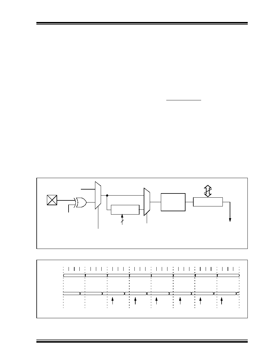
FIGURE 7-1:
TIMER0 BLOCK DIAGRAM
FIGURE 7-2:
TIMER0 TIMING: INTERNAL CLOCK/NO PRESCALE
Note 1:
TOCS, TOSE, PSA, PS<2:0> (OPTION<5:0>).
2: The prescaler is shared with Watchdog Timer (refer to Figure 7-6 for detailed block diagram).
GP2/TOCKI/
TOSE
0
1
0
AN2/INT
TOCS
FOSC/4
Programmable
Prescaler
Sync with
Internal
clocks
TMR0
(2 TCY delay)
Data Bus
8
PSA
PS<2:0>
Set interrupt
flag bit T0IF
on overflow
3
PC-1
Q1 Q2 Q3 Q4 Q1 Q2 Q3 Q4 Q1 Q2 Q3 Q4 Q1 Q2 Q3 Q4 Q1 Q2 Q3 Q4 Q1 Q2 Q3 Q4 Q1 Q2 Q3 Q4 Q1 Q2 Q3 Q4
PC
(Program
Counter)
Instruction
Fetch
TMR0
PC
PC+1
PC+2
PC+3
PC+4
PC+5
PC+6
T0
T0+1
T0+2
NT0
NT0+1
NT0+2
T0
MOVWF TMR0 MOVF TMR0,WMOVF TMR0,WMOVF TMR0,WMOVF TMR0,WMOVF TMR0,W
Write TMR0
executed
Read TMR0
reads NT0
Read TMR0
reads NT0
Read TMR0
reads NT0
Read TMR0
reads NT0 + 1
Read TMR0
reads NT0 + 2
Instruction
Executed
相关PDF资料 |
PDF描述 |
|---|---|
| PIC16F722-E/SO | IC PIC MCU FLASH 2KX14 28-SOIC |
| VI-22Y-IV-S | CONVERTER MOD DC/DC 3.3V 99W |
| PIC16C56AT-04/SS | IC MCU OTP 1KX12 20SSOP |
| VI-2TF-IX-S | CONVERTER MOD DC/DC 72V 75W |
| PIC18F24K22-E/SS | IC MCU 8BIT 16KB FLASH 28SSOP |
相关代理商/技术参数 |
参数描述 |
|---|---|
| PIC12LC671T-04/SM | 功能描述:8位微控制器 -MCU 1.75KB 128 RAM 6 I/O RoHS:否 制造商:Silicon Labs 核心:8051 处理器系列:C8051F39x 数据总线宽度:8 bit 最大时钟频率:50 MHz 程序存储器大小:16 KB 数据 RAM 大小:1 KB 片上 ADC:Yes 工作电源电压:1.8 V to 3.6 V 工作温度范围:- 40 C to + 105 C 封装 / 箱体:QFN-20 安装风格:SMD/SMT |
| PIC12LC671T-04I/MF | 功能描述:8位微控制器 -MCU .75KB 25 RAM 6 I/O RoHS:否 制造商:Silicon Labs 核心:8051 处理器系列:C8051F39x 数据总线宽度:8 bit 最大时钟频率:50 MHz 程序存储器大小:16 KB 数据 RAM 大小:1 KB 片上 ADC:Yes 工作电源电压:1.8 V to 3.6 V 工作温度范围:- 40 C to + 105 C 封装 / 箱体:QFN-20 安装风格:SMD/SMT |
| PIC12LC671T-04I/SM | 功能描述:8位微控制器 -MCU 1.75KB 128 RAM 6 I/O RoHS:否 制造商:Silicon Labs 核心:8051 处理器系列:C8051F39x 数据总线宽度:8 bit 最大时钟频率:50 MHz 程序存储器大小:16 KB 数据 RAM 大小:1 KB 片上 ADC:Yes 工作电源电压:1.8 V to 3.6 V 工作温度范围:- 40 C to + 105 C 封装 / 箱体:QFN-20 安装风格:SMD/SMT |
| PIC12LC672-04/P | 功能描述:8位微控制器 -MCU 3.5KB 128 RAM 6 I/O RoHS:否 制造商:Silicon Labs 核心:8051 处理器系列:C8051F39x 数据总线宽度:8 bit 最大时钟频率:50 MHz 程序存储器大小:16 KB 数据 RAM 大小:1 KB 片上 ADC:Yes 工作电源电压:1.8 V to 3.6 V 工作温度范围:- 40 C to + 105 C 封装 / 箱体:QFN-20 安装风格:SMD/SMT |
| PIC12LC672-04/SM | 功能描述:8位微控制器 -MCU 3.5KB 128 RAM 6 I/O RoHS:否 制造商:Silicon Labs 核心:8051 处理器系列:C8051F39x 数据总线宽度:8 bit 最大时钟频率:50 MHz 程序存储器大小:16 KB 数据 RAM 大小:1 KB 片上 ADC:Yes 工作电源电压:1.8 V to 3.6 V 工作温度范围:- 40 C to + 105 C 封装 / 箱体:QFN-20 安装风格:SMD/SMT |
发布紧急采购,3分钟左右您将得到回复。