- 您现在的位置:买卖IC网 > PDF目录11481 > PIC16C770T-I/SS (Microchip Technology)IC MCU OTP 2KX14 A/D PWM 20SSOP PDF资料下载
参数资料
| 型号: | PIC16C770T-I/SS |
| 厂商: | Microchip Technology |
| 文件页数: | 176/220页 |
| 文件大小: | 0K |
| 描述: | IC MCU OTP 2KX14 A/D PWM 20SSOP |
| 产品培训模块: | Asynchronous Stimulus |
| 标准包装: | 1,600 |
| 系列: | PIC® 16C |
| 核心处理器: | PIC |
| 芯体尺寸: | 8-位 |
| 速度: | 20MHz |
| 连通性: | I²C,SPI |
| 外围设备: | 欠压检测/复位,POR,PWM,WDT |
| 输入/输出数: | 15 |
| 程序存储器容量: | 3.5KB(2K x 14) |
| 程序存储器类型: | OTP |
| RAM 容量: | 256 x 8 |
| 电压 - 电源 (Vcc/Vdd): | 4 V ~ 5.5 V |
| 数据转换器: | A/D 6x12b |
| 振荡器型: | 内部 |
| 工作温度: | -40°C ~ 85°C |
| 封装/外壳: | 20-SSOP(0.209",5.30mm 宽) |
| 包装: | 带卷 (TR) |
| 配用: | XLT20SS1-1-ND - SOCKET TRANSITION 20DIP 20SSOP 309-1014-ND - ADAPTER 20-SSOP TO 20-DIP |
| 其它名称: | PIC16C770TI/SS |
第1页第2页第3页第4页第5页第6页第7页第8页第9页第10页第11页第12页第13页第14页第15页第16页第17页第18页第19页第20页第21页第22页第23页第24页第25页第26页第27页第28页第29页第30页第31页第32页第33页第34页第35页第36页第37页第38页第39页第40页第41页第42页第43页第44页第45页第46页第47页第48页第49页第50页第51页第52页第53页第54页第55页第56页第57页第58页第59页第60页第61页第62页第63页第64页第65页第66页第67页第68页第69页第70页第71页第72页第73页第74页第75页第76页第77页第78页第79页第80页第81页第82页第83页第84页第85页第86页第87页第88页第89页第90页第91页第92页第93页第94页第95页第96页第97页第98页第99页第100页第101页第102页第103页第104页第105页第106页第107页第108页第109页第110页第111页第112页第113页第114页第115页第116页第117页第118页第119页第120页第121页第122页第123页第124页第125页第126页第127页第128页第129页第130页第131页第132页第133页第134页第135页第136页第137页第138页第139页第140页第141页第142页第143页第144页第145页第146页第147页第148页第149页第150页第151页第152页第153页第154页第155页第156页第157页第158页第159页第160页第161页第162页第163页第164页第165页第166页第167页第168页第169页第170页第171页第172页第173页第174页第175页当前第176页第177页第178页第179页第180页第181页第182页第183页第184页第185页第186页第187页第188页第189页第190页第191页第192页第193页第194页第195页第196页第197页第198页第199页第200页第201页第202页第203页第204页第205页第206页第207页第208页第209页第210页第211页第212页第213页第214页第215页第216页第217页第218页第219页第220页
2002 Microchip Technology Inc.
DS41120B-page 57
PIC16C717/770/771
8.3.2
PWM DUTY CYCLE
The PWM duty cycle is specified by writing to the
CCPR1L register and to the CCP1CON<5:4> bits. Up
to 10-bit resolution is available. The CCPR1L contains
the eight MSbs and the CCP1CON<5:4> contains the
two LSbs. This 10-bit value is represented by
CCPR1L:CCP1CON<5:4>. The following equation is
used to calculate the PWM duty cycle in time:
PWM duty cycle
= (CCPR1L:CCP1CON<5:4>)
TOSC (TMR2 prescale value)
CCPR1L and CCP1CON<5:4> can be written to at any
time, but the duty cycle value is not latched into
CCPR1H until after a match between PR2 and TMR2
occurs (i.e., the period is complete). In PWM mode,
CCPR1H is a read-only register.
The CCPR1H register and a 2-bit internal latch are
used to double buffer the PWM duty cycle. This double
buffering is essential for glitchless PWM operation.
When the CCPR1H and 2-bit latch match TMR2 con-
catenated with an internal 2-bit Q clock or 2 bits of the
TMR2 prescaler, the CCP1 pin is cleared.
Maximum PWM resolution (bits) for a given PWM fre-
quency:
8.3.3
PWM OUTPUT CONFIGURATIONS
The PWM1M1 bits in the CCP1CON register allows
one of the following configurations:
Single output
Half-Bridge output
Full-Bridge output, Forward mode
Full-Bridge output, Reverse mode
In the Single Output mode, the RB3/CCP1/P1A pin is
used as the PWM output. Since the CCP1 output is
multiplexed with the PORTB<3> data latch, the
TRISB<3> bit must be cleared to make the CCP1 pin
an output.
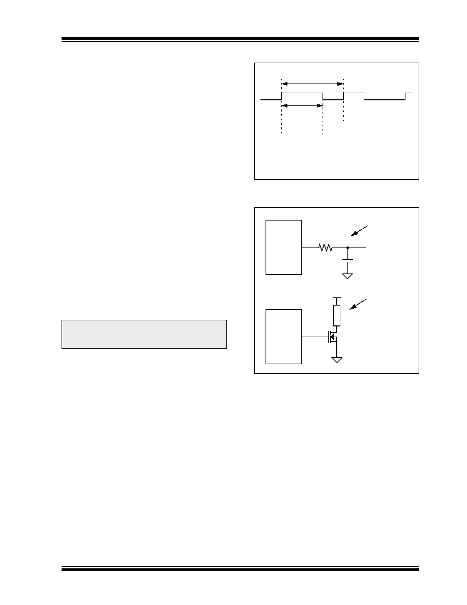
FIGURE 8-4:
SINGLE PWM OUTPUT
FIGURE 8-5:
EXAMPLE OF SINGLE
OUTPUT APPLICATION
In the Half-Bridge Output mode, two pins are used as
outputs. The RB3/CCP1/P1A pin has the PWM output
signal, while the RB5/SDO/P1B pin has the comple-
mentary PWM output signal. This mode can be used
for half-bridge applications, as shown on Figure 8-7, or
for full-bridge applications, where four power switches
are being modulated with two PWM signal.
Since the P1A and P1B outputs are multiplexed with
the PORTB<3> and PORTB<5> data latches, the
TRISB<3> and TRISB<5> bits must be cleared to con-
figure P1A and P1B as outputs.
In Half-Bridge Output mode, the programmable dead-
band delay can be used to prevent shoot-through cur-
rent in bridge power devices. See Section 8.3.5 for
more details of the deadband delay operations.
Note:
If the PWM duty cycle value is longer than
the PWM period, the CCP1 pin will not be
cleared.
FOSC
FPWM
---------------
log
2
()
log
-----------------------------bits
=
Period
Duty Cycle
(1)
Note 1: At this time, the TMR2 register is equal to the PR2 register.
CCP1(2)
2: Output signal is shown as asserted high.
C
PIC16C717/770/771
CCP1
R
Vout
Using PWM as
a D/A Converter
PIC16C717/770/771
CCP1
Using PWM to
Drive a Power
V+
L
O
A
D
Load
相关PDF资料 |
PDF描述 |
|---|---|
| PIC16LC711-04E/P | IC MCU OTP 1KX14 A/D 18DIP |
| VE-BNF-CU-F2 | CONVERTER MOD DC/DC 72V 200W |
| VE-BND-CU-F4 | CONVERTER MOD DC/DC 85V 200W |
| VE-BND-CU-F3 | CONVERTER MOD DC/DC 85V 200W |
| ADG508FBRNZ | IC MULTIPLEXER 8X1 16SOIC |
相关代理商/技术参数 |
参数描述 |
|---|---|
| PIC16C771/JW | 功能描述:8位微控制器 -MCU 7KB 256 RAM 16 I/O RoHS:否 制造商:Silicon Labs 核心:8051 处理器系列:C8051F39x 数据总线宽度:8 bit 最大时钟频率:50 MHz 程序存储器大小:16 KB 数据 RAM 大小:1 KB 片上 ADC:Yes 工作电源电压:1.8 V to 3.6 V 工作温度范围:- 40 C to + 105 C 封装 / 箱体:QFN-20 安装风格:SMD/SMT |
| PIC16C771/P | 功能描述:8位微控制器 -MCU 7KB 256 RAM 16 I/O RoHS:否 制造商:Silicon Labs 核心:8051 处理器系列:C8051F39x 数据总线宽度:8 bit 最大时钟频率:50 MHz 程序存储器大小:16 KB 数据 RAM 大小:1 KB 片上 ADC:Yes 工作电源电压:1.8 V to 3.6 V 工作温度范围:- 40 C to + 105 C 封装 / 箱体:QFN-20 安装风格:SMD/SMT |
| PIC16C771/P | 制造商:Microchip Technology Inc 功能描述:IC 8BIT CMOS MCU 16C771 DIP20 |
| PIC16C771/SO | 功能描述:8位微控制器 -MCU 7KB 256 RAM 16 I/O RoHS:否 制造商:Silicon Labs 核心:8051 处理器系列:C8051F39x 数据总线宽度:8 bit 最大时钟频率:50 MHz 程序存储器大小:16 KB 数据 RAM 大小:1 KB 片上 ADC:Yes 工作电源电压:1.8 V to 3.6 V 工作温度范围:- 40 C to + 105 C 封装 / 箱体:QFN-20 安装风格:SMD/SMT |
| PIC16C771/SS | 功能描述:8位微控制器 -MCU 7KB 256 RAM 16 I/O RoHS:否 制造商:Silicon Labs 核心:8051 处理器系列:C8051F39x 数据总线宽度:8 bit 最大时钟频率:50 MHz 程序存储器大小:16 KB 数据 RAM 大小:1 KB 片上 ADC:Yes 工作电源电压:1.8 V to 3.6 V 工作温度范围:- 40 C to + 105 C 封装 / 箱体:QFN-20 安装风格:SMD/SMT |
发布紧急采购,3分钟左右您将得到回复。