- 您现在的位置:买卖IC网 > PDF目录11481 > PIC16C770T-I/SS (Microchip Technology)IC MCU OTP 2KX14 A/D PWM 20SSOP PDF资料下载
参数资料
| 型号: | PIC16C770T-I/SS |
| 厂商: | Microchip Technology |
| 文件页数: | 184/220页 |
| 文件大小: | 0K |
| 描述: | IC MCU OTP 2KX14 A/D PWM 20SSOP |
| 产品培训模块: | Asynchronous Stimulus |
| 标准包装: | 1,600 |
| 系列: | PIC® 16C |
| 核心处理器: | PIC |
| 芯体尺寸: | 8-位 |
| 速度: | 20MHz |
| 连通性: | I²C,SPI |
| 外围设备: | 欠压检测/复位,POR,PWM,WDT |
| 输入/输出数: | 15 |
| 程序存储器容量: | 3.5KB(2K x 14) |
| 程序存储器类型: | OTP |
| RAM 容量: | 256 x 8 |
| 电压 - 电源 (Vcc/Vdd): | 4 V ~ 5.5 V |
| 数据转换器: | A/D 6x12b |
| 振荡器型: | 内部 |
| 工作温度: | -40°C ~ 85°C |
| 封装/外壳: | 20-SSOP(0.209",5.30mm 宽) |
| 包装: | 带卷 (TR) |
| 配用: | XLT20SS1-1-ND - SOCKET TRANSITION 20DIP 20SSOP 309-1014-ND - ADAPTER 20-SSOP TO 20-DIP |
| 其它名称: | PIC16C770TI/SS |
第1页第2页第3页第4页第5页第6页第7页第8页第9页第10页第11页第12页第13页第14页第15页第16页第17页第18页第19页第20页第21页第22页第23页第24页第25页第26页第27页第28页第29页第30页第31页第32页第33页第34页第35页第36页第37页第38页第39页第40页第41页第42页第43页第44页第45页第46页第47页第48页第49页第50页第51页第52页第53页第54页第55页第56页第57页第58页第59页第60页第61页第62页第63页第64页第65页第66页第67页第68页第69页第70页第71页第72页第73页第74页第75页第76页第77页第78页第79页第80页第81页第82页第83页第84页第85页第86页第87页第88页第89页第90页第91页第92页第93页第94页第95页第96页第97页第98页第99页第100页第101页第102页第103页第104页第105页第106页第107页第108页第109页第110页第111页第112页第113页第114页第115页第116页第117页第118页第119页第120页第121页第122页第123页第124页第125页第126页第127页第128页第129页第130页第131页第132页第133页第134页第135页第136页第137页第138页第139页第140页第141页第142页第143页第144页第145页第146页第147页第148页第149页第150页第151页第152页第153页第154页第155页第156页第157页第158页第159页第160页第161页第162页第163页第164页第165页第166页第167页第168页第169页第170页第171页第172页第173页第174页第175页第176页第177页第178页第179页第180页第181页第182页第183页当前第184页第185页第186页第187页第188页第189页第190页第191页第192页第193页第194页第195页第196页第197页第198页第199页第200页第201页第202页第203页第204页第205页第206页第207页第208页第209页第210页第211页第212页第213页第214页第215页第216页第217页第218页第219页第220页
PIC16C717/770/771
DS41120B-page 64
2002 Microchip Technology Inc.
8.3.7
SYSTEM IMPLEMENTATION
When the ECCP module is used in the PWM mode, the
application hardware must use the proper external pull-
up and/or pull-down resistors on the PWM output pins.
When the microcontroller powers up, all of the I/O pins
are in the high-impedance state. The external pull-up
and pull-down resistors must keep the power switch
devices in the off state until the microcontroller drives
the I/O pins with the proper signal levels, or activates
the PWM output(s).
8.3.8
START-UP CONSIDERATIONS
Prior to enabling the PWM outputs, the P1A, P1B, P1C
and P1D latches may not be in the proper states.
Enabling the TRISB bits for output at the same time
with the CCP module may cause damage to the power
switch devices. The CCP1 module must be enabled in
the proper Output mode with the TRISB bits enabled as
inputs. Once the CCP1 completes a full PWM cycle,
the P1A, P1B, P1C and P1D output latches are prop-
erly initialized. At this time, the TRISB bits can be
enabled for outputs to start driving the power switch
devices. The completion of a full PWM cycle is indi-
cated by the TMR2IF bit going from a ’0’ to a ’1’.
8.3.9
SET UP FOR PWM OPERATION
The following steps should be taken when configuring
the ECCP module for PWM operation:
1.
Configure the PWM module:
a)
Disable the CCP1/P1A, P1B, P1C and/or
P1D outputs by setting the respective
TRISB bits.
b)
Set the PWM period by loading the PR2
register.
c)
Set the PWM duty cycle by loading the
CCPR1L register and CCP1CON<5:4>
bits.
d)
Configure the ECCP module for the desired
PWM operation by loading the CCP1CON
register. With the CCP1M<3:0> bits select
the active high/low levels for each PWM
output. With the PWM1M<1:0> bits select
one of the available Output modes: Single,
Half-Bridge, Full-Bridge, Forward or Full-
Bridge Reverse.
e)
For Half-Bridge Output mode, set the dead-
band delay by loading the P1DEL register.
2.
Configure and start TMR2:
a)
Clear the TMR2 interrupt flag bit by clearing
the TMR2IF bit in the PIR1 register.
b)
Set the TMR2 prescale value by loading the
T2CKPS<1:0> bits in the T2CON register.
c)
Enable Timer2 by setting the TMR2ON bit
in the T2CON register.
3.
Enable PWM outputs after a new cycle has
started:
a)
Wait until TMR2 overflows (TMR2IF bit
becomes a ’1’). The new PWM cycle begins
here.
b)
Enable the CCP1/P1A, P1B, P1C and/or
P1D pin outputs by clearing the respective
TRISB bits.
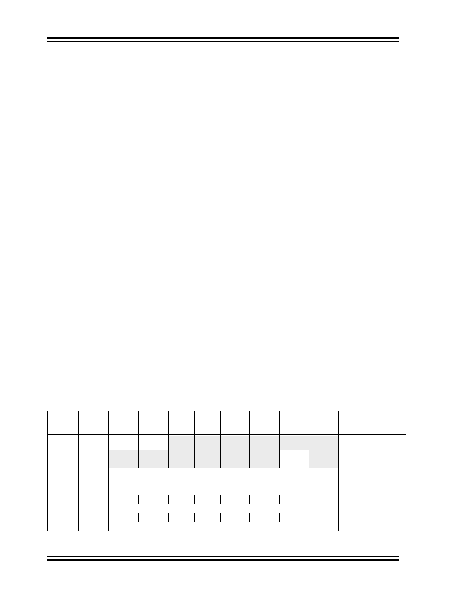
TABLE 8-3:
REGISTERS ASSOCIATED WITH PWM
Address
Name
Bit 7
Bit 6
Bit 5
Bit 4
Bit 3
Bit 2
Bit 1
Bit 0
Value on
POR,
BOR
Value on
all other
RESETS
0Bh, 8Bh,
10Bh, 18Bh
INTCON
GIE
PEIE
T0IE
INTE
RBIE
T0IF
INTF
RBIF
0000 000x
0000 000u
0Ch
PIR1
—
ADIF
—
SSPIF
CCP1IF
TMR2IF
TMR1IF
-0-- 0000
8Ch
PIE1
—
ADIE
—
SSPIE
CCP1IE
TMR2IE
TMR1IE
-0-- 0000
86h, 186h
TRISB
PORTB Data Direction Register
1111 1111
11h
TMR2
Timer2 register
0000 0000
92h
PR2
Timer2 period register
1111 1111
12h
T2CON
—
TOUTPS3 TOUTPS2 TOUTPS1 TOUTPS0
TMR2ON
T2CKPS1
T2CKPS0
-000 0000
15h
CCPR1L
Capture/Compare/PWM register1 (LSB)
xxxx xxxx
uuuu uuuu
17h
CCP1CON PWM1M1
PWM1M0
DC1B1
DC1B0
CCP1M3
CCP1M2
CCP1M1
CCP1M0
0000 0000
97h
P1DEL
PWM1 Delay value
0000 0000
Legend:
x = unknown, u = unchanged, - = unimplemented read as '0'. Shaded cells are not used by ECCP module in PWM mode.
相关PDF资料 |
PDF描述 |
|---|---|
| PIC16LC711-04E/P | IC MCU OTP 1KX14 A/D 18DIP |
| VE-BNF-CU-F2 | CONVERTER MOD DC/DC 72V 200W |
| VE-BND-CU-F4 | CONVERTER MOD DC/DC 85V 200W |
| VE-BND-CU-F3 | CONVERTER MOD DC/DC 85V 200W |
| ADG508FBRNZ | IC MULTIPLEXER 8X1 16SOIC |
相关代理商/技术参数 |
参数描述 |
|---|---|
| PIC16C771/JW | 功能描述:8位微控制器 -MCU 7KB 256 RAM 16 I/O RoHS:否 制造商:Silicon Labs 核心:8051 处理器系列:C8051F39x 数据总线宽度:8 bit 最大时钟频率:50 MHz 程序存储器大小:16 KB 数据 RAM 大小:1 KB 片上 ADC:Yes 工作电源电压:1.8 V to 3.6 V 工作温度范围:- 40 C to + 105 C 封装 / 箱体:QFN-20 安装风格:SMD/SMT |
| PIC16C771/P | 功能描述:8位微控制器 -MCU 7KB 256 RAM 16 I/O RoHS:否 制造商:Silicon Labs 核心:8051 处理器系列:C8051F39x 数据总线宽度:8 bit 最大时钟频率:50 MHz 程序存储器大小:16 KB 数据 RAM 大小:1 KB 片上 ADC:Yes 工作电源电压:1.8 V to 3.6 V 工作温度范围:- 40 C to + 105 C 封装 / 箱体:QFN-20 安装风格:SMD/SMT |
| PIC16C771/P | 制造商:Microchip Technology Inc 功能描述:IC 8BIT CMOS MCU 16C771 DIP20 |
| PIC16C771/SO | 功能描述:8位微控制器 -MCU 7KB 256 RAM 16 I/O RoHS:否 制造商:Silicon Labs 核心:8051 处理器系列:C8051F39x 数据总线宽度:8 bit 最大时钟频率:50 MHz 程序存储器大小:16 KB 数据 RAM 大小:1 KB 片上 ADC:Yes 工作电源电压:1.8 V to 3.6 V 工作温度范围:- 40 C to + 105 C 封装 / 箱体:QFN-20 安装风格:SMD/SMT |
| PIC16C771/SS | 功能描述:8位微控制器 -MCU 7KB 256 RAM 16 I/O RoHS:否 制造商:Silicon Labs 核心:8051 处理器系列:C8051F39x 数据总线宽度:8 bit 最大时钟频率:50 MHz 程序存储器大小:16 KB 数据 RAM 大小:1 KB 片上 ADC:Yes 工作电源电压:1.8 V to 3.6 V 工作温度范围:- 40 C to + 105 C 封装 / 箱体:QFN-20 安装风格:SMD/SMT |
发布紧急采购,3分钟左右您将得到回复。