- 您现在的位置:买卖IC网 > PDF目录11481 > PIC16C770T-I/SS (Microchip Technology)IC MCU OTP 2KX14 A/D PWM 20SSOP PDF资料下载
参数资料
| 型号: | PIC16C770T-I/SS |
| 厂商: | Microchip Technology |
| 文件页数: | 182/220页 |
| 文件大小: | 0K |
| 描述: | IC MCU OTP 2KX14 A/D PWM 20SSOP |
| 产品培训模块: | Asynchronous Stimulus |
| 标准包装: | 1,600 |
| 系列: | PIC® 16C |
| 核心处理器: | PIC |
| 芯体尺寸: | 8-位 |
| 速度: | 20MHz |
| 连通性: | I²C,SPI |
| 外围设备: | 欠压检测/复位,POR,PWM,WDT |
| 输入/输出数: | 15 |
| 程序存储器容量: | 3.5KB(2K x 14) |
| 程序存储器类型: | OTP |
| RAM 容量: | 256 x 8 |
| 电压 - 电源 (Vcc/Vdd): | 4 V ~ 5.5 V |
| 数据转换器: | A/D 6x12b |
| 振荡器型: | 内部 |
| 工作温度: | -40°C ~ 85°C |
| 封装/外壳: | 20-SSOP(0.209",5.30mm 宽) |
| 包装: | 带卷 (TR) |
| 配用: | XLT20SS1-1-ND - SOCKET TRANSITION 20DIP 20SSOP 309-1014-ND - ADAPTER 20-SSOP TO 20-DIP |
| 其它名称: | PIC16C770TI/SS |
第1页第2页第3页第4页第5页第6页第7页第8页第9页第10页第11页第12页第13页第14页第15页第16页第17页第18页第19页第20页第21页第22页第23页第24页第25页第26页第27页第28页第29页第30页第31页第32页第33页第34页第35页第36页第37页第38页第39页第40页第41页第42页第43页第44页第45页第46页第47页第48页第49页第50页第51页第52页第53页第54页第55页第56页第57页第58页第59页第60页第61页第62页第63页第64页第65页第66页第67页第68页第69页第70页第71页第72页第73页第74页第75页第76页第77页第78页第79页第80页第81页第82页第83页第84页第85页第86页第87页第88页第89页第90页第91页第92页第93页第94页第95页第96页第97页第98页第99页第100页第101页第102页第103页第104页第105页第106页第107页第108页第109页第110页第111页第112页第113页第114页第115页第116页第117页第118页第119页第120页第121页第122页第123页第124页第125页第126页第127页第128页第129页第130页第131页第132页第133页第134页第135页第136页第137页第138页第139页第140页第141页第142页第143页第144页第145页第146页第147页第148页第149页第150页第151页第152页第153页第154页第155页第156页第157页第158页第159页第160页第161页第162页第163页第164页第165页第166页第167页第168页第169页第170页第171页第172页第173页第174页第175页第176页第177页第178页第179页第180页第181页当前第182页第183页第184页第185页第186页第187页第188页第189页第190页第191页第192页第193页第194页第195页第196页第197页第198页第199页第200页第201页第202页第203页第204页第205页第206页第207页第208页第209页第210页第211页第212页第213页第214页第215页第216页第217页第218页第219页第220页
PIC16C717/770/771
DS41120B-page 62
2002 Microchip Technology Inc.
8.3.5
PROGRAMMABLE DEADBAND
DELAY
In half-bridge or full-bridge applications, driven by half-
bridge outputs (see Figure 8-7), the power switches
normally require longer time to turn off than to turn on.
If both the upper and lower power switches are
switched at the same time (one turned on, and the
other turned off), both switches will be on for a short
period of time, until one switch completely turns off.
During this time, a very high current, called shoot-
through current, will flow through both power switches,
shorting the bridge supply. To avoid this potentially
destructive shoot-through current from flowing during
switching, turning on the power switch is normally
delayed to allow the other switch to completely turn off.
In the Half-Bridge Output mode, a digitally program-
mable deadband delay is available to avoid shoot-
through current from destroying the bridge power
switches. The delay occurs at the signal transition from
the non-active state to the active state. See Figure 8-6
for illustration. The P1DEL register sets the amount of
delay.
REGISTER 8-2:
PWM DELAY REGISTER (P1DEL: 97H)
8.3.6
DIRECTION CHANGE IN FULL-
BRIDGE OUTPUT MODE
In the Full-Bridge Output mode, the PWM1M1 bit in the
CCP1CON register allows user to control the Forward/
Reverse direction. When the application firmware
changes this direction control bit, the ECCP module will
assume the new direction on the next PWM cycle. The
current PWM cycle still continues, however, the non-
modulated outputs, P1A and P1C signals, will transition
to the new direction TOSC, 4
TOSC or 16TOSC (for
Timer2 prescale T2CKRS<1:0> = 00, 01 and 1x
respectively) earlier, before the end of the period. Dur-
ing this transition cycle, the modulated outputs, P1B
and P1D, will go to the inactive state. See Figure 8-10
for illustration.
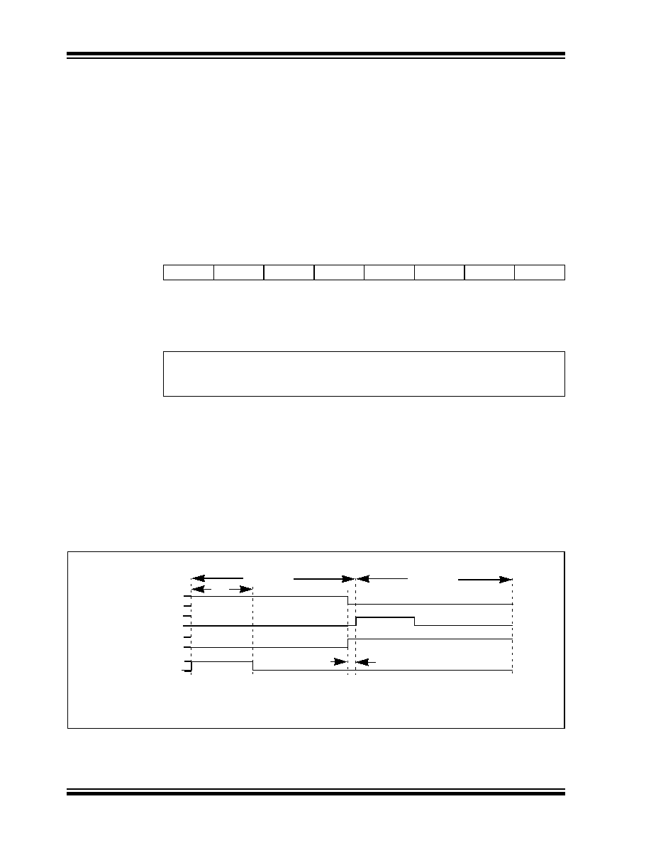
FIGURE 8-10: PWM DIRECTION CHANGE
R/W-0
P1DEL7
P1DEL6
P1DEL5
P1DEL4
P1DEL3
P1DEL2
P1DEL1
P1DEL0
bit 7
bit 0
bit 7-0
P1DEL<7:0>: PWM Delay Count for Half-Bridge Output Mode: Number of FOSC/4 (Tosc
4)
cycles between the P1A transition and the P1B transition.
Legend:
R = Readable bit
W = Writable bit
U = Unimplemented bit, read as ‘0’
- n = Value at POR
’1’ = Bit is set
’0’ = Bit is cleared
x = Bit is unknown
DC
PERIOD
SIGNAL
P1A (Active High)
Note 1:
The Direction bit in the ECCP Control Register (CCP1CON<PWM1M1>) is written anytime during the PWM cycle.
2:
The P1A and P1C signals switch TOSC, 4*Tosc or 16*TOSC, depending on the Timer2 prescaler value, earlier when
changing direction. The modulated P1B and P1D signals are inactive at this time.
(1)
PERIOD
(2)
P1D (Active High)
P1C (Active High)
P1B (Active High)
相关PDF资料 |
PDF描述 |
|---|---|
| PIC16LC711-04E/P | IC MCU OTP 1KX14 A/D 18DIP |
| VE-BNF-CU-F2 | CONVERTER MOD DC/DC 72V 200W |
| VE-BND-CU-F4 | CONVERTER MOD DC/DC 85V 200W |
| VE-BND-CU-F3 | CONVERTER MOD DC/DC 85V 200W |
| ADG508FBRNZ | IC MULTIPLEXER 8X1 16SOIC |
相关代理商/技术参数 |
参数描述 |
|---|---|
| PIC16C771/JW | 功能描述:8位微控制器 -MCU 7KB 256 RAM 16 I/O RoHS:否 制造商:Silicon Labs 核心:8051 处理器系列:C8051F39x 数据总线宽度:8 bit 最大时钟频率:50 MHz 程序存储器大小:16 KB 数据 RAM 大小:1 KB 片上 ADC:Yes 工作电源电压:1.8 V to 3.6 V 工作温度范围:- 40 C to + 105 C 封装 / 箱体:QFN-20 安装风格:SMD/SMT |
| PIC16C771/P | 功能描述:8位微控制器 -MCU 7KB 256 RAM 16 I/O RoHS:否 制造商:Silicon Labs 核心:8051 处理器系列:C8051F39x 数据总线宽度:8 bit 最大时钟频率:50 MHz 程序存储器大小:16 KB 数据 RAM 大小:1 KB 片上 ADC:Yes 工作电源电压:1.8 V to 3.6 V 工作温度范围:- 40 C to + 105 C 封装 / 箱体:QFN-20 安装风格:SMD/SMT |
| PIC16C771/P | 制造商:Microchip Technology Inc 功能描述:IC 8BIT CMOS MCU 16C771 DIP20 |
| PIC16C771/SO | 功能描述:8位微控制器 -MCU 7KB 256 RAM 16 I/O RoHS:否 制造商:Silicon Labs 核心:8051 处理器系列:C8051F39x 数据总线宽度:8 bit 最大时钟频率:50 MHz 程序存储器大小:16 KB 数据 RAM 大小:1 KB 片上 ADC:Yes 工作电源电压:1.8 V to 3.6 V 工作温度范围:- 40 C to + 105 C 封装 / 箱体:QFN-20 安装风格:SMD/SMT |
| PIC16C771/SS | 功能描述:8位微控制器 -MCU 7KB 256 RAM 16 I/O RoHS:否 制造商:Silicon Labs 核心:8051 处理器系列:C8051F39x 数据总线宽度:8 bit 最大时钟频率:50 MHz 程序存储器大小:16 KB 数据 RAM 大小:1 KB 片上 ADC:Yes 工作电源电压:1.8 V to 3.6 V 工作温度范围:- 40 C to + 105 C 封装 / 箱体:QFN-20 安装风格:SMD/SMT |
发布紧急采购,3分钟左右您将得到回复。