- 您现在的位置:买卖IC网 > PDF目录299771 > PIC16F676-E/SL 8-BIT, FLASH, 20 MHz, RISC MICROCONTROLLER, PDSO14 PDF资料下载
参数资料
| 型号: | PIC16F676-E/SL |
| 元件分类: | 微控制器/微处理器 |
| 英文描述: | 8-BIT, FLASH, 20 MHz, RISC MICROCONTROLLER, PDSO14 |
| 封装: | 3.90 MM, LEAD FREE, PLASTIC, SOIC-14 |
| 文件页数: | 73/132页 |
| 文件大小: | 1344K |
| 代理商: | PIC16F676-E/SL |
第1页第2页第3页第4页第5页第6页第7页第8页第9页第10页第11页第12页第13页第14页第15页第16页第17页第18页第19页第20页第21页第22页第23页第24页第25页第26页第27页第28页第29页第30页第31页第32页第33页第34页第35页第36页第37页第38页第39页第40页第41页第42页第43页第44页第45页第46页第47页第48页第49页第50页第51页第52页第53页第54页第55页第56页第57页第58页第59页第60页第61页第62页第63页第64页第65页第66页第67页第68页第69页第70页第71页第72页当前第73页第74页第75页第76页第77页第78页第79页第80页第81页第82页第83页第84页第85页第86页第87页第88页第89页第90页第91页第92页第93页第94页第95页第96页第97页第98页第99页第100页第101页第102页第103页第104页第105页第106页第107页第108页第109页第110页第111页第112页第113页第114页第115页第116页第117页第118页第119页第120页第121页第122页第123页第124页第125页第126页第127页第128页第129页第130页第131页第132页
2010 Microchip Technology Inc.
DS40039F-page 45
PIC16F630/676
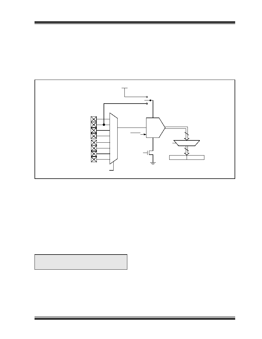
7.0
ANALOG-TO-DIGITAL
CONVERTER (A/D) MODULE
(PIC16F676 ONLY)
The Analog-to-Digital Converter (ADC) allows conver-
sion of an analog input signal to a 10-bit binary repre-
sentation of that signal. The PIC16F676 has eight
analog inputs, multiplexed into one sample and hold
circuit. The output of the sample and hold is connected
to the input of the converter. The converter generates a
binary result via successive approximation and stores
the result in a 10-bit register. The voltage reference
used in the conversion is software selectable to either
shows the block diagram of the A/D on the PIC16F676.
FIGURE 7-1:
A/D BLOCK DIAGRAM
7.1
A/D Configuration and Operation
There are three registers available to control the
functionality of the A/D module:
1.
ADCON0 (Register 7-1)
2.
ADCON1 (Register 7-2)
3.
ANSEL (Register 7-3)
7.1.1
ANALOG PORT PINS
The ANS7:ANS0 bits (ANSEL<7:0>) and the TRISA
bits control the operation of the A/D port pins. Set the
corresponding TRISA bits to set the pin output driver to
its high-impedance state. Likewise, set the correspond-
ing ANS bit to disable the digital input buffer.
7.1.2
CHANNEL SELECTION
There are eight analog channels on the PIC16F676,
AN0
through
AN7.
The
CHS2:CHS0
bits
(ADCON0<4:2>) control which channel is connected to
the sample and hold circuit.
7.1.3
VOLTAGE REFERENCE
There are two options for the voltage reference to the
A/D converter: either VDD is used, or an analog voltage
applied to VREF is used. The VCFG bit (ADCON0<6>)
controls the voltage reference selection. If VCFG is set,
then the voltage on the VREF pin is the reference;
otherwise, VDD is the reference.
7.1.4
CONVERSION CLOCK
The A/D conversion cycle requires 11 TAD. The source
of the conversion clock is software selectable via the
ADCS bits (ADCON1<6:4>). There are seven possible
clock options:
FOSC/2
FOSC/4
FOSC/8
FOSC/16
FOSC/32
FOSC/64
FRC (dedicated internal oscillator)
For correct conversion, the A/D conversion clock
(1/TAD) must be selected to ensure a minimum TAD of
1.6
selected frequencies.
RA0/AN0
ADC
RA1/AN1/VREF
RA2/AN2
RC0/AN4
VDD
VREF
ADON
GO/DONE
VCFG = 1
VCFG = 0
CHS2:CHS0
ADRESH ADRESL
10
ADFM
VSS
RC1/AN5
RC2/AN6
RC3/AN7
RA4/AN3
Note:
Analog voltages on any pin that is defined
as a digital input may cause the input
buffer to conduct excess current.
相关PDF资料 |
PDF描述 |
|---|---|
| PIC16LC433E/P | 8-BIT, OTPROM, 4 MHz, RISC MICROCONTROLLER, PDIP18 |
| PIC16LC556-04/SS | 8-BIT, OTPROM, 4 MHz, RISC MICROCONTROLLER, PDSO20 |
| PIC16LC662T-04/L | 8-BIT, OTPROM, 4 MHz, RISC MICROCONTROLLER, PQCC44 |
| PIC16C662T-20I/P | 8-BIT, OTPROM, 20 MHz, RISC MICROCONTROLLER, PDIP40 |
| PIC16C662T-20I/L | 8-BIT, OTPROM, 20 MHz, RISC MICROCONTROLLER, PQCC44 |
相关代理商/技术参数 |
参数描述 |
|---|---|
| PIC16F676-I/ML | 功能描述:8位微控制器 -MCU 1.75 KB 64 RAM 12I/O RoHS:否 制造商:Silicon Labs 核心:8051 处理器系列:C8051F39x 数据总线宽度:8 bit 最大时钟频率:50 MHz 程序存储器大小:16 KB 数据 RAM 大小:1 KB 片上 ADC:Yes 工作电源电压:1.8 V to 3.6 V 工作温度范围:- 40 C to + 105 C 封装 / 箱体:QFN-20 安装风格:SMD/SMT |
| PIC16F676-I/P | 功能描述:8位微控制器 -MCU 1.75KB 64 RAM 12 I/O Ind Temp PDIP14 RoHS:否 制造商:Silicon Labs 核心:8051 处理器系列:C8051F39x 数据总线宽度:8 bit 最大时钟频率:50 MHz 程序存储器大小:16 KB 数据 RAM 大小:1 KB 片上 ADC:Yes 工作电源电压:1.8 V to 3.6 V 工作温度范围:- 40 C to + 105 C 封装 / 箱体:QFN-20 安装风格:SMD/SMT |
| PIC16F676-I/P | 制造商:Microchip Technology Inc 功能描述:IC 8BIT FLASH MCU 16F676 DIP14 |
| PIC16F676-I/SL | 功能描述:8位微控制器 -MCU 1.75KB 64 RAM 12 I/O Ind Temp SOIC14 RoHS:否 制造商:Silicon Labs 核心:8051 处理器系列:C8051F39x 数据总线宽度:8 bit 最大时钟频率:50 MHz 程序存储器大小:16 KB 数据 RAM 大小:1 KB 片上 ADC:Yes 工作电源电压:1.8 V to 3.6 V 工作温度范围:- 40 C to + 105 C 封装 / 箱体:QFN-20 安装风格:SMD/SMT |
| PIC16F676-I/SL | 制造商:Microchip Technology Inc 功能描述:8BIT FLASH MCU SMD 16F676 SOIC14 |
发布紧急采购,3分钟左右您将得到回复。