- 您现在的位置:买卖IC网 > PDF目录11472 > PIC16LC62B-04/SP (Microchip Technology)IC MCU OTP 2KX14 PWM 28DIP PDF资料下载
参数资料
| 型号: | PIC16LC62B-04/SP |
| 厂商: | Microchip Technology |
| 文件页数: | 37/120页 |
| 文件大小: | 0K |
| 描述: | IC MCU OTP 2KX14 PWM 28DIP |
| 产品培训模块: | Asynchronous Stimulus |
| 标准包装: | 15 |
| 系列: | PIC® 16C |
| 核心处理器: | PIC |
| 芯体尺寸: | 8-位 |
| 速度: | 4MHz |
| 连通性: | I²C,SPI |
| 外围设备: | 欠压检测/复位,POR,PWM,WDT |
| 输入/输出数: | 22 |
| 程序存储器容量: | 3.5KB(2K x 14) |
| 程序存储器类型: | OTP |
| RAM 容量: | 128 x 8 |
| 电压 - 电源 (Vcc/Vdd): | 2.5 V ~ 5.5 V |
| 振荡器型: | 外部 |
| 工作温度: | 0°C ~ 70°C |
| 封装/外壳: | 28-DIP(0.300",7.62mm) |
| 包装: | 管件 |
第1页第2页第3页第4页第5页第6页第7页第8页第9页第10页第11页第12页第13页第14页第15页第16页第17页第18页第19页第20页第21页第22页第23页第24页第25页第26页第27页第28页第29页第30页第31页第32页第33页第34页第35页第36页当前第37页第38页第39页第40页第41页第42页第43页第44页第45页第46页第47页第48页第49页第50页第51页第52页第53页第54页第55页第56页第57页第58页第59页第60页第61页第62页第63页第64页第65页第66页第67页第68页第69页第70页第71页第72页第73页第74页第75页第76页第77页第78页第79页第80页第81页第82页第83页第84页第85页第86页第87页第88页第89页第90页第91页第92页第93页第94页第95页第96页第97页第98页第99页第100页第101页第102页第103页第104页第105页第106页第107页第108页第109页第110页第111页第112页第113页第114页第115页第116页第117页第118页第119页第120页
PIC16C62B/72A
1999 Microchip Technology Inc.
Preliminary
DS35008B-page 23
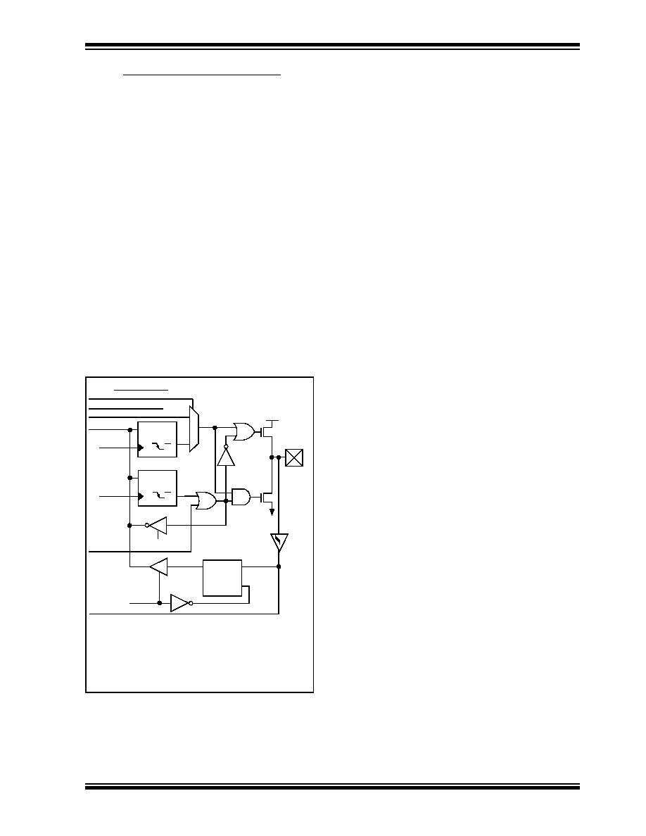
3.3
PORTC and the TRISC Register
PORTC is an 8-bit wide bi-directional port. The corre-
sponding data direction register is TRISC. Setting a
TRISC bit (=1) will make the corresponding PORTC pin
an input, (i.e., put the corresponding output driver in a
hi-impedance mode). Clearing a TRISC bit (=0) will
make the corresponding PORTC pin an output, (i.e.,
put the contents of the output latch on the selected pin).
PORTC is multiplexed with several peripheral functions
(Table 3-5). PORTC pins have Schmitt Trigger input
buffers.
When enabling peripheral functions, care should be
taken in defining TRIS bits for each PORTC pin. Some
peripherals override the TRIS bit to make a pin an out-
put, while other peripherals override the TRIS bit to
make a pin an input. Since the TRIS bit override maybe
in effect while the peripheral is enabled, read-modify-
write instructions (BSF, BCF, XORWF) with TRISC as
destination should be avoided. The user should refer to
the corresponding peripheral section for the correct
TRIS bit settings.
FIGURE 3-5:
PORTC BLOCK DIAGRAM
(PERIPHERAL OUTPUT
OVERRIDE)
PORT/PERIPHERAL Select(2)
Data Bus
WR
PORT
WR
TRIS
RD
Data Latch
TRIS Latch
RD TRIS
Schmitt
Trigger
Q
D
Q
CK
QD
EN
Peripheral Data Out
0
1
Q
D
Q
CK
P
N
VDD
VSS
PORT
Peripheral
OE(3)
Peripheral input
I/O
pin(1)
Note 1:
I/O pins have diode protection to VDD and VSS.
2: Port/Peripheral select signal selects between port
data and peripheral output.
3: Peripheral OE (output enable) is only activated if
peripheral select is active.
相关PDF资料 |
PDF描述 |
|---|---|
| VI-B21-IW-S | CONVERTER MOD DC/DC 12V 100W |
| VI-B6V-CU-F3 | CONVERTER MOD DC/DC 5.8V 200W |
| VI-23Z-IV | CONVERTER MOD DC/DC 2V 60W |
| VI-B6V-CU-F2 | CONVERTER MOD DC/DC 5.8V 200W |
| VI-B6M-CU-F4 | CONVERTER MOD DC/DC 10V 200W |
相关代理商/技术参数 |
参数描述 |
|---|---|
| PIC16LC62BT-04/SO | 功能描述:8位微控制器 -MCU 3.5KB 128 RAM 22 I/O RoHS:否 制造商:Silicon Labs 核心:8051 处理器系列:C8051F39x 数据总线宽度:8 bit 最大时钟频率:50 MHz 程序存储器大小:16 KB 数据 RAM 大小:1 KB 片上 ADC:Yes 工作电源电压:1.8 V to 3.6 V 工作温度范围:- 40 C to + 105 C 封装 / 箱体:QFN-20 安装风格:SMD/SMT |
| PIC16LC62BT-04/SS | 功能描述:8位微控制器 -MCU 3.5KB 128 RAM 22 I/O RoHS:否 制造商:Silicon Labs 核心:8051 处理器系列:C8051F39x 数据总线宽度:8 bit 最大时钟频率:50 MHz 程序存储器大小:16 KB 数据 RAM 大小:1 KB 片上 ADC:Yes 工作电源电压:1.8 V to 3.6 V 工作温度范围:- 40 C to + 105 C 封装 / 箱体:QFN-20 安装风格:SMD/SMT |
| PIC16LC62BT-04I/ML | 功能描述:8位微控制器 -MCU 3.5KB 128 RAM 22 I/O RoHS:否 制造商:Silicon Labs 核心:8051 处理器系列:C8051F39x 数据总线宽度:8 bit 最大时钟频率:50 MHz 程序存储器大小:16 KB 数据 RAM 大小:1 KB 片上 ADC:Yes 工作电源电压:1.8 V to 3.6 V 工作温度范围:- 40 C to + 105 C 封装 / 箱体:QFN-20 安装风格:SMD/SMT |
| PIC16LC62BT-04I/SO | 功能描述:8位微控制器 -MCU 3.5KB 128 RAM 22 I/O RoHS:否 制造商:Silicon Labs 核心:8051 处理器系列:C8051F39x 数据总线宽度:8 bit 最大时钟频率:50 MHz 程序存储器大小:16 KB 数据 RAM 大小:1 KB 片上 ADC:Yes 工作电源电压:1.8 V to 3.6 V 工作温度范围:- 40 C to + 105 C 封装 / 箱体:QFN-20 安装风格:SMD/SMT |
| PIC16LC62BT-04I/SS | 功能描述:8位微控制器 -MCU 3.5KB 128 RAM 22 I/O RoHS:否 制造商:Silicon Labs 核心:8051 处理器系列:C8051F39x 数据总线宽度:8 bit 最大时钟频率:50 MHz 程序存储器大小:16 KB 数据 RAM 大小:1 KB 片上 ADC:Yes 工作电源电压:1.8 V to 3.6 V 工作温度范围:- 40 C to + 105 C 封装 / 箱体:QFN-20 安装风格:SMD/SMT |
发布紧急采购,3分钟左右您将得到回复。