- 您现在的位置:买卖IC网 > PDF目录11513 > PIC16LC716-04I/P (Microchip Technology)IC MCU OTP 2KX14 A/D PWM 18DIP PDF资料下载
参数资料
| 型号: | PIC16LC716-04I/P |
| 厂商: | Microchip Technology |
| 文件页数: | 32/106页 |
| 文件大小: | 0K |
| 描述: | IC MCU OTP 2KX14 A/D PWM 18DIP |
| 产品培训模块: | Asynchronous Stimulus |
| 标准包装: | 25 |
| 系列: | PIC® 16C |
| 核心处理器: | PIC |
| 芯体尺寸: | 8-位 |
| 速度: | 4MHz |
| 外围设备: | 欠压检测/复位,POR,PWM,WDT |
| 输入/输出数: | 13 |
| 程序存储器容量: | 3.5KB(2K x 14) |
| 程序存储器类型: | OTP |
| RAM 容量: | 128 x 8 |
| 电压 - 电源 (Vcc/Vdd): | 2.5 V ~ 5.5 V |
| 数据转换器: | A/D 4x8b |
| 振荡器型: | 外部 |
| 工作温度: | -40°C ~ 85°C |
| 封装/外壳: | 18-DIP(0.300",7.62mm) |
| 包装: | 管件 |
第1页第2页第3页第4页第5页第6页第7页第8页第9页第10页第11页第12页第13页第14页第15页第16页第17页第18页第19页第20页第21页第22页第23页第24页第25页第26页第27页第28页第29页第30页第31页当前第32页第33页第34页第35页第36页第37页第38页第39页第40页第41页第42页第43页第44页第45页第46页第47页第48页第49页第50页第51页第52页第53页第54页第55页第56页第57页第58页第59页第60页第61页第62页第63页第64页第65页第66页第67页第68页第69页第70页第71页第72页第73页第74页第75页第76页第77页第78页第79页第80页第81页第82页第83页第84页第85页第86页第87页第88页第89页第90页第91页第92页第93页第94页第95页第96页第97页第98页第99页第100页第101页第102页第103页第104页第105页第106页
2005 Microchip Technology Inc.
DS41106B-page 29
PIC16C712/716
4.0
TIMER0 MODULE
The Timer0 module timer/counter has the following
features:
8-bit timer/counter
Readable and writable
Internal or external clock select
Edge select for external clock
8-bit software programmable prescaler
Interrupt on overflow from FFh to 00h
Figure 4-1 is a simplified block diagram of the Timer0
module.
Additional information on timer modules is available in
the
PICmicro
Mid-Range
Reference
Manual,
(DS33023).
4.1
Timer0 Operation
Timer0 can operate as a timer or as a counter.
Timer mode is selected by clearing bit T0CS
(OPTION_REG<5>). In timer mode, the Timer0 mod-
ule will increment every instruction cycle (without pres-
caler). If the TMR0 register is written, the increment is
inhibited for the following two instruction cycles. The
user can work around this by writing an adjusted value
to the TMR0 register.
Counter mode is selected by setting bit T0CS
(OPTION_REG<5>). In Counter mode, Timer0 will
increment on every rising or falling edge of pin RA4/
T0CKI. The incrementing edge is determined by the
Timer0
Source
Edge
Select
bit
T0SE
(OPTION_REG<4>). Clearing bit T0SE selects the
rising edge. Restrictions on the external clock input are
discussed below.
When an external clock input is used for Timer0, it must
meet certain requirements. The requirements ensure
the external clock can be synchronized with the internal
phase clock (TOSC). Also, there is a delay in the actual
incrementing of Timer0 after synchronization.
Additional information on external clock requirements
is available in the PICmicro Mid-Range Reference
Manual, (DS33023).
4.2
Prescaler
An 8-bit counter is available as a prescaler for the
Timer0 module or as a postscaler for the Watchdog
Timer, respectively (Figure 4-2). For simplicity, this
counter is being referred to as “prescaler” throughout
this data sheet. Note that there is only one prescaler
available,
which
is
mutually
exclusively
shared
between the Timer0 module and the Watchdog Timer.
Thus, a prescaler assignment for the Timer0 module
means that there is no prescaler for the Watchdog
Timer and vice-versa.
The prescaler is not readable or writable.
The PSA and PS2:PS0 bits (OPTION_REG<3:0>)
determine the prescaler assignment and prescale ratio.
Clearing bit PSA will assign the prescaler to the Timer0
module. When the prescaler is assigned to the Timer0
module, prescale values of 1:2, 1:4, ..., 1:256 are
selectable.
Setting bit PSA will assign the prescaler to the Watch-
dog Timer (WDT). When the prescaler is assigned to
the WDT, prescale values of 1:1, 1:2, ..., 1:128 are
selectable.
When assigned to the Timer0 module, all instructions
writing to the TMR0 register (e.g., CLRF 1, MOVWF 1,
BSF
1,x
....etc.) will clear the prescaler. When
assigned to WDT, a CLRWDT instruction will clear the
prescaler along with the WDT.
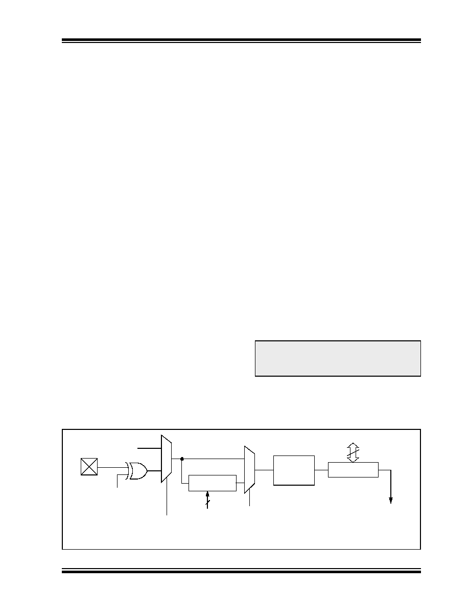
FIGURE 4-1:
TIMER0 BLOCK DIAGRAM
Note:
Writing to TMR0 when the prescaler is
assigned to Timer0 will clear the prescaler
count, but will not change the prescaler
assignment.
Note 1: T0CS, T0SE, PSA, PS2:PS0 (OPTION_REG<5:0>).
2: The prescaler is shared with Watchdog Timer (refer to Figure 4-2 for detailed block diagram).
RA4/T0CKI
T0SE(1)
0
1
0
pin
T0CS(1)
FOSC/4
Programmable
Prescaler(2)
Sync with
Internal
clocks
TMR0
PSout
(2-cycle delay)
PSout
Data Bus
8
PSA(1)
PS2, PS1, PS0(1)
Set Interrupt
Flag bit T0IF
on overflow
3
相关PDF资料 |
PDF描述 |
|---|---|
| PIC16LC712-04I/SS | IC MCU OTP 1KX14 A/D PWM 20SSOP |
| DG411LDQ-T1-E3 | IC SWITCH QUAD SPST LV 16-TSSOP |
| PIC16LC57C-04/SS | IC MCU OTP 2KX12 28SSOP |
| VE-B0X-IY-B1 | CONVERTER MOD DC/DC 5.2V 50W |
| PIC16LC57C-04I/SP | IC MCU OTP 2KX12 28DIP |
相关代理商/技术参数 |
参数描述 |
|---|---|
| PIC16LC716T-04/SO | 功能描述:8位微控制器 -MCU 3.5KB 128 RAM 13 I/O RoHS:否 制造商:Silicon Labs 核心:8051 处理器系列:C8051F39x 数据总线宽度:8 bit 最大时钟频率:50 MHz 程序存储器大小:16 KB 数据 RAM 大小:1 KB 片上 ADC:Yes 工作电源电压:1.8 V to 3.6 V 工作温度范围:- 40 C to + 105 C 封装 / 箱体:QFN-20 安装风格:SMD/SMT |
| PIC16LC716T-04/SS | 功能描述:8位微控制器 -MCU 3.5KB 128 RAM 13 I/O RoHS:否 制造商:Silicon Labs 核心:8051 处理器系列:C8051F39x 数据总线宽度:8 bit 最大时钟频率:50 MHz 程序存储器大小:16 KB 数据 RAM 大小:1 KB 片上 ADC:Yes 工作电源电压:1.8 V to 3.6 V 工作温度范围:- 40 C to + 105 C 封装 / 箱体:QFN-20 安装风格:SMD/SMT |
| PIC16LC716T-04I/SO | 功能描述:8位微控制器 -MCU 3.5KB 128 RAM 13 I/O RoHS:否 制造商:Silicon Labs 核心:8051 处理器系列:C8051F39x 数据总线宽度:8 bit 最大时钟频率:50 MHz 程序存储器大小:16 KB 数据 RAM 大小:1 KB 片上 ADC:Yes 工作电源电压:1.8 V to 3.6 V 工作温度范围:- 40 C to + 105 C 封装 / 箱体:QFN-20 安装风格:SMD/SMT |
| PIC16LC716T-04I/SS | 功能描述:8位微控制器 -MCU 3.5KB 128 RAM 13 I/O RoHS:否 制造商:Silicon Labs 核心:8051 处理器系列:C8051F39x 数据总线宽度:8 bit 最大时钟频率:50 MHz 程序存储器大小:16 KB 数据 RAM 大小:1 KB 片上 ADC:Yes 工作电源电压:1.8 V to 3.6 V 工作温度范围:- 40 C to + 105 C 封装 / 箱体:QFN-20 安装风格:SMD/SMT |
| PIC16LC717/P | 功能描述:8位微控制器 -MCU 3.5KB 256 RAM 16 I/O RoHS:否 制造商:Silicon Labs 核心:8051 处理器系列:C8051F39x 数据总线宽度:8 bit 最大时钟频率:50 MHz 程序存储器大小:16 KB 数据 RAM 大小:1 KB 片上 ADC:Yes 工作电源电压:1.8 V to 3.6 V 工作温度范围:- 40 C to + 105 C 封装 / 箱体:QFN-20 安装风格:SMD/SMT |
发布紧急采购,3分钟左右您将得到回复。