- 您现在的位置:买卖IC网 > PDF目录11513 > PIC16LC716-04I/P (Microchip Technology)IC MCU OTP 2KX14 A/D PWM 18DIP PDF资料下载
参数资料
| 型号: | PIC16LC716-04I/P |
| 厂商: | Microchip Technology |
| 文件页数: | 46/106页 |
| 文件大小: | 0K |
| 描述: | IC MCU OTP 2KX14 A/D PWM 18DIP |
| 产品培训模块: | Asynchronous Stimulus |
| 标准包装: | 25 |
| 系列: | PIC® 16C |
| 核心处理器: | PIC |
| 芯体尺寸: | 8-位 |
| 速度: | 4MHz |
| 外围设备: | 欠压检测/复位,POR,PWM,WDT |
| 输入/输出数: | 13 |
| 程序存储器容量: | 3.5KB(2K x 14) |
| 程序存储器类型: | OTP |
| RAM 容量: | 128 x 8 |
| 电压 - 电源 (Vcc/Vdd): | 2.5 V ~ 5.5 V |
| 数据转换器: | A/D 4x8b |
| 振荡器型: | 外部 |
| 工作温度: | -40°C ~ 85°C |
| 封装/外壳: | 18-DIP(0.300",7.62mm) |
| 包装: | 管件 |
第1页第2页第3页第4页第5页第6页第7页第8页第9页第10页第11页第12页第13页第14页第15页第16页第17页第18页第19页第20页第21页第22页第23页第24页第25页第26页第27页第28页第29页第30页第31页第32页第33页第34页第35页第36页第37页第38页第39页第40页第41页第42页第43页第44页第45页当前第46页第47页第48页第49页第50页第51页第52页第53页第54页第55页第56页第57页第58页第59页第60页第61页第62页第63页第64页第65页第66页第67页第68页第69页第70页第71页第72页第73页第74页第75页第76页第77页第78页第79页第80页第81页第82页第83页第84页第85页第86页第87页第88页第89页第90页第91页第92页第93页第94页第95页第96页第97页第98页第99页第100页第101页第102页第103页第104页第105页第106页
PIC16C712/716
DS41106B-page 42
2005 Microchip Technology Inc.
7.3
PWM Mode
In Pulse Width Modulation (PWM) mode, the CCP1 pin
produces up to a 10-bit resolution PWM output. Since
the CCP1 pin is multiplexed with the PORTB data latch,
the TRISCCP<2> bit must be cleared to make the
CCP1 pin an output.
Figure 7-5 shows a simplified block diagram of the
CCP module in PWM mode.
For a step by step procedure on how to set up the CCP
module for PWM operation, see Section 7.3.3 “Set-
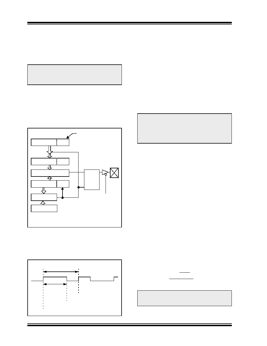
FIGURE 7-5:
SIMPLIFIED PWM BLOCK
DIAGRAM
A PWM output (Figure 7-6) has a time base (period)
and a time that the output stays high (duty cycle). The
frequency of the PWM is the inverse of the period (1/
period).
FIGURE 7-6:
PWM OUTPUT
7.3.1
PWM PERIOD
The PWM period is specified by writing to the PR2
register. The PWM period can be calculated using the
following formula:
PWM period = [(PR2) + 1] 4 TOSC
(TMR2 prescale value)
PWM frequency is defined as 1 / [PWM period].
When TMR2 is equal to PR2, the following three events
occur on the next increment cycle:
TMR2 is cleared
The CCP1 pin is set (exception: if PWM duty
cycle = 0%, the CCP1 pin will not be set)
The PWM duty cycle is latched from CCPR1L into
CCPR1H
7.3.2
PWM DUTY CYCLE
The PWM duty cycle is specified by writing to the
CCPR1L register and to the CCP1CON<5:4> bits. Up
to 10-bit resolution is available. The CCPR1L contains
the eight MSbs and the CCP1CON<5:4> contains the
two LSbs. This 10-bit value is represented by
CCPR1L:CCP1CON<5:4>. The following equation is
used to calculate the PWM duty cycle in time:
PWM duty cycle = (CCPR1L:CCP1CON<5:4>)
Tosc (TMR2 prescale value)
CCPR1L and CCP1CON<5:4> can be written to at any
time, but the duty cycle value is not latched into
CCPR1H until after a match between PR2 and TMR2
occurs (i.e., the period is complete). In PWM mode,
CCPR1H is a read-only register.
The CCPR1H register and a 2-bit internal latch are
used to double buffer the PWM duty cycle. This double
buffering is essential for glitchless PWM operation.
When the CCPR1H and 2-bit latch match TMR2
concatenated with an internal 2-bit Q clock or 2 bits of
the TMR2 prescaler, the CCP1 pin is cleared.
Maximum PWM resolution (bits) for a given PWM
frequency:
For an example PWM period and duty cycle calcula-
tion, see the PICmicro Mid-Range Reference Manual,
(DS33023).
Note:
Clearing the CCP1CON register will force
the CCP1 PWM output latch to the default
low level. This is neither the PORTB I/O
data latch nor the DATACCP latch.
CCPR1L
CCPR1H (Slave)
Comparator
TMR2
Comparator
PR2
(Note 1)
R
Q
S
Duty cycle registers
CCP1CON<5:4>
Clear Timer,
CCP1 pin and
latch D.C.
TRISCCP<2>
RB3/CCP1
Note 1: 8-bit timer is concatenated with 2-bit internal Q clock
or 2 bits of the prescaler to create 10-bit time base.
Period = PR2+1
Duty Cycle
TMR2 = PR2
TMR2 = Duty Cycle (CCPR1H)
TMR2 = PR2
Note:
The Timer2 postscaler (see Section 6.0
“Timer2 Module”) is not used in the
determination of the PWM frequency. The
postscaler could be used to have a servo
update rate at a different frequency than
the PWM output.
Note:
If the PWM duty cycle value is longer than
the PWM period the CCP1 pin will not be
cleared.
log
( FPWM
log(2)
FOSC
)
bits
=
相关PDF资料 |
PDF描述 |
|---|---|
| PIC16LC712-04I/SS | IC MCU OTP 1KX14 A/D PWM 20SSOP |
| DG411LDQ-T1-E3 | IC SWITCH QUAD SPST LV 16-TSSOP |
| PIC16LC57C-04/SS | IC MCU OTP 2KX12 28SSOP |
| VE-B0X-IY-B1 | CONVERTER MOD DC/DC 5.2V 50W |
| PIC16LC57C-04I/SP | IC MCU OTP 2KX12 28DIP |
相关代理商/技术参数 |
参数描述 |
|---|---|
| PIC16LC716T-04/SO | 功能描述:8位微控制器 -MCU 3.5KB 128 RAM 13 I/O RoHS:否 制造商:Silicon Labs 核心:8051 处理器系列:C8051F39x 数据总线宽度:8 bit 最大时钟频率:50 MHz 程序存储器大小:16 KB 数据 RAM 大小:1 KB 片上 ADC:Yes 工作电源电压:1.8 V to 3.6 V 工作温度范围:- 40 C to + 105 C 封装 / 箱体:QFN-20 安装风格:SMD/SMT |
| PIC16LC716T-04/SS | 功能描述:8位微控制器 -MCU 3.5KB 128 RAM 13 I/O RoHS:否 制造商:Silicon Labs 核心:8051 处理器系列:C8051F39x 数据总线宽度:8 bit 最大时钟频率:50 MHz 程序存储器大小:16 KB 数据 RAM 大小:1 KB 片上 ADC:Yes 工作电源电压:1.8 V to 3.6 V 工作温度范围:- 40 C to + 105 C 封装 / 箱体:QFN-20 安装风格:SMD/SMT |
| PIC16LC716T-04I/SO | 功能描述:8位微控制器 -MCU 3.5KB 128 RAM 13 I/O RoHS:否 制造商:Silicon Labs 核心:8051 处理器系列:C8051F39x 数据总线宽度:8 bit 最大时钟频率:50 MHz 程序存储器大小:16 KB 数据 RAM 大小:1 KB 片上 ADC:Yes 工作电源电压:1.8 V to 3.6 V 工作温度范围:- 40 C to + 105 C 封装 / 箱体:QFN-20 安装风格:SMD/SMT |
| PIC16LC716T-04I/SS | 功能描述:8位微控制器 -MCU 3.5KB 128 RAM 13 I/O RoHS:否 制造商:Silicon Labs 核心:8051 处理器系列:C8051F39x 数据总线宽度:8 bit 最大时钟频率:50 MHz 程序存储器大小:16 KB 数据 RAM 大小:1 KB 片上 ADC:Yes 工作电源电压:1.8 V to 3.6 V 工作温度范围:- 40 C to + 105 C 封装 / 箱体:QFN-20 安装风格:SMD/SMT |
| PIC16LC717/P | 功能描述:8位微控制器 -MCU 3.5KB 256 RAM 16 I/O RoHS:否 制造商:Silicon Labs 核心:8051 处理器系列:C8051F39x 数据总线宽度:8 bit 最大时钟频率:50 MHz 程序存储器大小:16 KB 数据 RAM 大小:1 KB 片上 ADC:Yes 工作电源电压:1.8 V to 3.6 V 工作温度范围:- 40 C to + 105 C 封装 / 箱体:QFN-20 安装风格:SMD/SMT |
发布紧急采购,3分钟左右您将得到回复。