- 您现在的位置:买卖IC网 > PDF目录1964 > PIC16LF1933-I/MV (Microchip Technology)IC MCU 8BIT 7KB FLASH 28UQFN PDF资料下载
参数资料
| 型号: | PIC16LF1933-I/MV |
| 厂商: | Microchip Technology |
| 文件页数: | 149/295页 |
| 文件大小: | 0K |
| 描述: | IC MCU 8BIT 7KB FLASH 28UQFN |
| 产品培训模块: | 8-bit PIC® Microcontroller Portfolio |
| 标准包装: | 91 |
| 系列: | PIC® XLP™ 16F |
| 核心处理器: | PIC |
| 芯体尺寸: | 8-位 |
| 速度: | 32MHz |
| 连通性: | I²C,LIN,SPI,UART/USART |
| 外围设备: | 欠压检测/复位,LCD,POR,PWM,WDT |
| 输入/输出数: | 25 |
| 程序存储器容量: | 7KB(4K x 14) |
| 程序存储器类型: | 闪存 |
| EEPROM 大小: | 256 x 8 |
| RAM 容量: | 256 x 8 |
| 电压 - 电源 (Vcc/Vdd): | 1.8 V ~ 3.6 V |
| 数据转换器: | A/D 11x10b |
| 振荡器型: | 内部 |
| 工作温度: | -40°C ~ 85°C |
| 封装/外壳: | 28-UFQFN 裸露焊盘 |
| 包装: | 管件 |
第1页第2页第3页第4页第5页第6页第7页第8页第9页第10页第11页第12页第13页第14页第15页第16页第17页第18页第19页第20页第21页第22页第23页第24页第25页第26页第27页第28页第29页第30页第31页第32页第33页第34页第35页第36页第37页第38页第39页第40页第41页第42页第43页第44页第45页第46页第47页第48页第49页第50页第51页第52页第53页第54页第55页第56页第57页第58页第59页第60页第61页第62页第63页第64页第65页第66页第67页第68页第69页第70页第71页第72页第73页第74页第75页第76页第77页第78页第79页第80页第81页第82页第83页第84页第85页第86页第87页第88页第89页第90页第91页第92页第93页第94页第95页第96页第97页第98页第99页第100页第101页第102页第103页第104页第105页第106页第107页第108页第109页第110页第111页第112页第113页第114页第115页第116页第117页第118页第119页第120页第121页第122页第123页第124页第125页第126页第127页第128页第129页第130页第131页第132页第133页第134页第135页第136页第137页第138页第139页第140页第141页第142页第143页第144页第145页第146页第147页第148页当前第149页第150页第151页第152页第153页第154页第155页第156页第157页第158页第159页第160页第161页第162页第163页第164页第165页第166页第167页第168页第169页第170页第171页第172页第173页第174页第175页第176页第177页第178页第179页第180页第181页第182页第183页第184页第185页第186页第187页第188页第189页第190页第191页第192页第193页第194页第195页第196页第197页第198页第199页第200页第201页第202页第203页第204页第205页第206页第207页第208页第209页第210页第211页第212页第213页第214页第215页第216页第217页第218页第219页第220页第221页第222页第223页第224页第225页第226页第227页第228页第229页第230页第231页第232页第233页第234页第235页第236页第237页第238页第239页第240页第241页第242页第243页第244页第245页第246页第247页第248页第249页第250页第251页第252页第253页第254页第255页第256页第257页第258页第259页第260页第261页第262页第263页第264页第265页第266页第267页第268页第269页第270页第271页第272页第273页第274页第275页第276页第277页第278页第279页第280页第281页第282页第283页第284页第285页第286页第287页第288页第289页第290页第291页第292页第293页第294页第295页
PIC18FXX8
DS41159E-page 230
2006 Microchip Technology Inc.
19.5
Message Reception
19.5.1
RECEIVE MESSAGE BUFFERING
The PIC18FXX8 includes two full receive buffers with
multiple acceptance filters for each. There is also a
separate Message Assembly Buffer (MAB) which acts
as a third receive buffer (see Figure 19-4).
19.5.2
RECEIVE BUFFERS
Of the three receive buffers, the MAB is always commit-
ted to receiving the next message from the bus. The
remaining two receive buffers are called RXB0 and
RXB1 and can receive a complete message from the
protocol engine. The MCU can access one buffer while
the other buffer is available for message reception or
holding a previously received message.
The MAB assembles all messages received. These
messages will be transferred to the RXBn buffers only
if the acceptance filter criteria are met.
When a message is moved into either of the receive
buffers, the appropriate RXBnIF bit is set. This bit must
be cleared by the MCU when it has completed process-
ing the message in the buffer in order to allow a new
message to be received into the buffer. This bit
provides a positive lockout to ensure that the MCU has
finished with the message before the PIC18FXX8
attempts to load a new message into the receive buffer.
If the RXBnIE bit is set, an interrupt will be generated to
indicate that a valid message has been received.
19.5.3
RECEIVE PRIORITY
RXB0 is the higher priority buffer and has two message
acceptance filters associated with it. RXB1 is the lower
priority buffer and has four acceptance filters associ-
ated with it. The lower number of acceptance filters
makes the match on RXB0 more restrictive and implies
a higher priority for that buffer. Additionally, the
RXB0CON register can be configured such if RXB0
contains a valid message and another valid message is
received, an overflow error will not occur and the new
message will be moved into RXB1 regardless of the
acceptance criteria of RXB1. There are also two
programmable acceptance filter masks available, one
for each receive buffer (see Section 19.6 “Message
When a message is received, bits <3:0> of the
RXBnCON register will indicate the acceptance filter
number that enabled reception and whether the
received message is a remote transfer request.
The RXM bits set special Receive modes. Normally,
these bits are set to ‘00’ to enable reception of all valid
messages as determined by the appropriate accep-
tance filters. In this case, the determination of whether
or not to receive standard or extended messages is
determined by the EXIDE bit in the Acceptance Filter
register. If the RXM bits are set to ‘01’ or ‘10’, the
receiver will accept only messages with standard or
extended identifiers, respectively. If an acceptance
filter has the EXIDE bit set, such that it does not corre-
spond with the RXM mode, that acceptance filter is
rendered useless. These two modes of RXM bits can
be used in systems where it is known that only standard
or extended messages will be on the bus. If the RXM
bits are set to ‘11’, the buffer will receive all messages
regardless of the values of the acceptance filters. Also,
if a message has an error before the end of frame, that
portion of the message assembled in the MAB before
the error frame will be loaded into the buffer. This mode
has some value in debugging a CAN system and would
not be used in an actual system environment.
19.5.4
TIME-STAMPING
The CAN module can be programmed to generate a
time-stamp for every message that is received. When
enabled, the module generates a capture signal for
CCP1 which in turns captures the value of either
Timer1 or Timer3. This value can be used as the
message time-stamp.
To use the time-stamp capability, the CANCAP bit
(CIOCAN<4>) must be set. This replaces the capture
input for CCP1 with the signal generated from the CAN
module. In addition, CCP1CON<3:0> must be set to
‘0011’ to enable the CCP special event trigger for CAN
events.
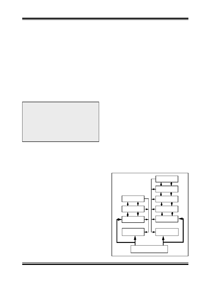
FIGURE 19-4:
RECEIVE BUFFER BLOCK
DIAGRAM
Note:
The entire contents of the MAB are moved
into the receive buffer once a message is
accepted. This means that regardless of
the
type
of
identifier
(standard
or
extended) and the number of data bytes
received, the entire receive buffer is over-
written with the MAB contents. Therefore,
the contents of all registers in the buffer
must be assumed to have been modified
when any message is received.
Acceptance Mask
RXM0
Acceptance Filter
RXF0
Acceptance Filter
RXF1
Message Assembly Buffer
Acceptance Filter
RXM2
Acceptance Filter
RXF3
Acceptance Filter
RXF4
Acceptance Filter
RXF5
Acceptance Mask
RXM1
RXB0
RXB1
Accept
Data and
Identifier
Data and
Identifier
相关PDF资料 |
PDF描述 |
|---|---|
| PIC16LF1936-I/MV | IC MCU 8BIT 14KB FLASH 28UQFN |
| PIC16LF1937-E/MV | IC PIC MCU FLASH 512KX14 40UQFN |
| PIC16LF1939-I/P | IC MCU 8BIT FLASH 40-DIP |
| PIC16LF1946T-I/MR | MCU 8BIT 14KB FLASH 64QFN |
| PIC16LF1947T-I/MR | MCU 8BIT 28KB FLASH 64QFN |
相关代理商/技术参数 |
参数描述 |
|---|---|
| PIC16LF1933T-I/ML | 功能描述:8位微控制器 -MCU 7KB Flash 1.8-5.5V 256B RAM 256B EEPROM RoHS:否 制造商:Silicon Labs 核心:8051 处理器系列:C8051F39x 数据总线宽度:8 bit 最大时钟频率:50 MHz 程序存储器大小:16 KB 数据 RAM 大小:1 KB 片上 ADC:Yes 工作电源电压:1.8 V to 3.6 V 工作温度范围:- 40 C to + 105 C 封装 / 箱体:QFN-20 安装风格:SMD/SMT |
| PIC16LF1933T-I/MV | 功能描述:8位微控制器 -MCU 7KB FL 256BRAM 256B EE LCD nanoWatt XLP RoHS:否 制造商:Silicon Labs 核心:8051 处理器系列:C8051F39x 数据总线宽度:8 bit 最大时钟频率:50 MHz 程序存储器大小:16 KB 数据 RAM 大小:1 KB 片上 ADC:Yes 工作电源电压:1.8 V to 3.6 V 工作温度范围:- 40 C to + 105 C 封装 / 箱体:QFN-20 安装风格:SMD/SMT |
| PIC16LF1933T-I/SO | 功能描述:8位微控制器 -MCU 7KB Flash 1.8-5.5V 256B RAM 256B EEPROM RoHS:否 制造商:Silicon Labs 核心:8051 处理器系列:C8051F39x 数据总线宽度:8 bit 最大时钟频率:50 MHz 程序存储器大小:16 KB 数据 RAM 大小:1 KB 片上 ADC:Yes 工作电源电压:1.8 V to 3.6 V 工作温度范围:- 40 C to + 105 C 封装 / 箱体:QFN-20 安装风格:SMD/SMT |
| PIC16LF1933T-I/SS | 功能描述:8位微控制器 -MCU 7KB Flash 1.8-5.5V 256B RAM 256B EEPROM RoHS:否 制造商:Silicon Labs 核心:8051 处理器系列:C8051F39x 数据总线宽度:8 bit 最大时钟频率:50 MHz 程序存储器大小:16 KB 数据 RAM 大小:1 KB 片上 ADC:Yes 工作电源电压:1.8 V to 3.6 V 工作温度范围:- 40 C to + 105 C 封装 / 箱体:QFN-20 安装风格:SMD/SMT |
| PIC16LF1934-E/ML | 功能描述:8位微控制器 -MCU 7KB Flash, 256B RAM 256B EE LCD 1.8-5.5V RoHS:否 制造商:Silicon Labs 核心:8051 处理器系列:C8051F39x 数据总线宽度:8 bit 最大时钟频率:50 MHz 程序存储器大小:16 KB 数据 RAM 大小:1 KB 片上 ADC:Yes 工作电源电压:1.8 V to 3.6 V 工作温度范围:- 40 C to + 105 C 封装 / 箱体:QFN-20 安装风格:SMD/SMT |
发布紧急采购,3分钟左右您将得到回复。