- 您现在的位置:买卖IC网 > PDF目录11560 > PIC16LF627A-I/ML (Microchip Technology)IC MCU FLASH 1KX14 EEPROM 28QFN PDF资料下载
参数资料
| 型号: | PIC16LF627A-I/ML |
| 厂商: | Microchip Technology |
| 文件页数: | 12/180页 |
| 文件大小: | 0K |
| 描述: | IC MCU FLASH 1KX14 EEPROM 28QFN |
| 产品培训模块: | Asynchronous Stimulus |
| 标准包装: | 61 |
| 系列: | PIC® 16F |
| 核心处理器: | PIC |
| 芯体尺寸: | 8-位 |
| 速度: | 20MHz |
| 连通性: | UART/USART |
| 外围设备: | 欠压检测/复位,POR,PWM,WDT |
| 输入/输出数: | 16 |
| 程序存储器容量: | 1.75KB(1K x 14) |
| 程序存储器类型: | 闪存 |
| EEPROM 大小: | 128 x 8 |
| RAM 容量: | 224 x 8 |
| 电压 - 电源 (Vcc/Vdd): | 2 V ~ 5.5 V |
| 振荡器型: | 内部 |
| 工作温度: | -40°C ~ 85°C |
| 封装/外壳: | 28-VQFN 裸露焊盘 |
| 包装: | 管件 |
第1页第2页第3页第4页第5页第6页第7页第8页第9页第10页第11页当前第12页第13页第14页第15页第16页第17页第18页第19页第20页第21页第22页第23页第24页第25页第26页第27页第28页第29页第30页第31页第32页第33页第34页第35页第36页第37页第38页第39页第40页第41页第42页第43页第44页第45页第46页第47页第48页第49页第50页第51页第52页第53页第54页第55页第56页第57页第58页第59页第60页第61页第62页第63页第64页第65页第66页第67页第68页第69页第70页第71页第72页第73页第74页第75页第76页第77页第78页第79页第80页第81页第82页第83页第84页第85页第86页第87页第88页第89页第90页第91页第92页第93页第94页第95页第96页第97页第98页第99页第100页第101页第102页第103页第104页第105页第106页第107页第108页第109页第110页第111页第112页第113页第114页第115页第116页第117页第118页第119页第120页第121页第122页第123页第124页第125页第126页第127页第128页第129页第130页第131页第132页第133页第134页第135页第136页第137页第138页第139页第140页第141页第142页第143页第144页第145页第146页第147页第148页第149页第150页第151页第152页第153页第154页第155页第156页第157页第158页第159页第160页第161页第162页第163页第164页第165页第166页第167页第168页第169页第170页第171页第172页第173页第174页第175页第176页第177页第178页第179页第180页
2009 Microchip Technology Inc.
DS40044G-page 109
PIC16F627A/628A/648A
14.5
Interrupts
The PIC16F627A/628A/648A has 10 sources of
interrupt:
External Interrupt RB0/INT
TMR0 Overflow Interrupt
PORTB Change Interrupts (pins RB<7:4>)
Comparator Interrupt
USART Interrupt TX
USART Interrupt RX
CCP Interrupt
TMR1 Overflow Interrupt
TMR2 Match Interrupt
Data EEPROM Interrupt
The Interrupt Control register (INTCON) records
individual interrupt requests in flag bits. It also has
individual and global interrupt enable bits.
A Global Interrupt Enable bit, GIE (INTCON<7>)
enables (if set) all un-masked interrupts or disables (if
cleared) all interrupts. Individual interrupts can be
disabled through their corresponding enable bits in
INTCON register. GIE is cleared on Reset.
The “return-from-interrupt” instruction, RETFIE, exits
interrupt routine as well as sets the GIE bit, which re-
enables RB0/INT interrupts.
The INT pin interrupt, the RB port change interrupt and
the TMR0 overflow interrupt flags are contained in the
INTCON register.
The peripheral interrupt flag is contained in the special
register PIR1. The corresponding interrupt enable bit is
contained in special registers PIE1.
When an interrupt is responded to, the GIE is cleared
to disable any further interrupt, the return address is
pushed into the stack and the PC is loaded with 0004h.
Once in the interrupt service routine, the source(s) of
the interrupt can be determined by polling the interrupt
flag bits. The interrupt flag bit(s) must be cleared in
software before re-enabling interrupts to avoid RB0/
INT recursive interrupts.
For external interrupt events, such as the INT pin or
PORTB change interrupt, the interrupt latency will be
three or four instruction cycles. The exact latency
depends when the interrupt event occurs (Figure 14-15).
The latency is the same for one or two-cycle instructions.
Once in the interrupt service routine, the source(s) of the
interrupt can be determined by polling the interrupt flag
bits. The interrupt flag bit(s) must be cleared in software
before re-enabling interrupts to avoid multiple interrupt
requests.
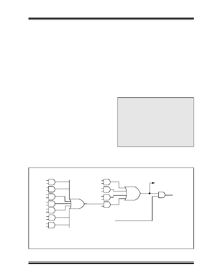
FIGURE 14-14:
INTERRUPT LOGIC
Note 1:
Individual interrupt flag bits are set
regardless
of
the
status
of
their
corresponding mask bit or the GIE bit.
2:
When an instruction that clears the GIE
bit is executed, any interrupts that were
pending for execution in the next cycle
are ignored. The CPU will execute a NOP
in the cycle immediately following the
instruction which clears the GIE bit. The
interrupts which were ignored are still
pending to be serviced when the GIE bit
is set again.
TMR2IF
TMR2IE
CCP1IF
CCP1IE
CMIF
CMIE
TXIF
TXIE
RCIF
RCIE
T0IF
T0IE
INTF
INTE
RBIF
RBIE
GIE
PEIE
Wake-up (if in Sleep mode)(1)
Interrupt to CPU
EEIE
EEIF
TMR1IF
TMR1IE
Note 1:
Some peripherals depend upon the system clock for operation. Since the system clock is
suspended during Sleep, only those peripherals which do not depend upon the system
clock will wake the part from Sleep. See Section 14.8.1 “Wake-up from Sleep”.
相关PDF资料 |
PDF描述 |
|---|---|
| PIC16C621A-40/SO | IC MCU OTP 1KX14 COMP 18SOIC |
| PIC16LC620AT-04/SS | IC MCU OTP 512X14 COMP 20SSOP |
| PIC16LC620AT-04I/SS | IC MCU OTP 512X14 COMP 20SSOP |
| VI-243-IX-S | CONVERTER MOD DC/DC 24V 75W |
| VE-2TR-IX-S | CONVERTER MOD DC/DC 7.5V 75W |
相关代理商/技术参数 |
参数描述 |
|---|---|
| PIC16LF627AT-I/ML | 功能描述:8位微控制器 -MCU 1.75KB 224 RAM 16I/O Ind Temp QFN28 RoHS:否 制造商:Silicon Labs 核心:8051 处理器系列:C8051F39x 数据总线宽度:8 bit 最大时钟频率:50 MHz 程序存储器大小:16 KB 数据 RAM 大小:1 KB 片上 ADC:Yes 工作电源电压:1.8 V to 3.6 V 工作温度范围:- 40 C to + 105 C 封装 / 箱体:QFN-20 安装风格:SMD/SMT |
| PIC16LF627AT-I/SO | 功能描述:8位微控制器 -MCU 1.75KB 224 RAM 16I/O Ind Temp SOIC18 RoHS:否 制造商:Silicon Labs 核心:8051 处理器系列:C8051F39x 数据总线宽度:8 bit 最大时钟频率:50 MHz 程序存储器大小:16 KB 数据 RAM 大小:1 KB 片上 ADC:Yes 工作电源电压:1.8 V to 3.6 V 工作温度范围:- 40 C to + 105 C 封装 / 箱体:QFN-20 安装风格:SMD/SMT |
| PIC16LF627AT-I/SS | 功能描述:8位微控制器 -MCU 1.75KB 224 RAM 16I/O Ind Temp SSOP20 RoHS:否 制造商:Silicon Labs 核心:8051 处理器系列:C8051F39x 数据总线宽度:8 bit 最大时钟频率:50 MHz 程序存储器大小:16 KB 数据 RAM 大小:1 KB 片上 ADC:Yes 工作电源电压:1.8 V to 3.6 V 工作温度范围:- 40 C to + 105 C 封装 / 箱体:QFN-20 安装风格:SMD/SMT |
| PIC16LF627-I/SS | 制造商:Microchip Technology Inc 功能描述: |
| PIC16LF627T-04/SO | 功能描述:8位微控制器 -MCU 1.75KB 224 RAM 16I/O 4MHz SOIC18 RoHS:否 制造商:Silicon Labs 核心:8051 处理器系列:C8051F39x 数据总线宽度:8 bit 最大时钟频率:50 MHz 程序存储器大小:16 KB 数据 RAM 大小:1 KB 片上 ADC:Yes 工作电源电压:1.8 V to 3.6 V 工作温度范围:- 40 C to + 105 C 封装 / 箱体:QFN-20 安装风格:SMD/SMT |
发布紧急采购,3分钟左右您将得到回复。