- 您现在的位置:买卖IC网 > PDF目录11560 > PIC16LF627A-I/ML (Microchip Technology)IC MCU FLASH 1KX14 EEPROM 28QFN PDF资料下载
参数资料
| 型号: | PIC16LF627A-I/ML |
| 厂商: | Microchip Technology |
| 文件页数: | 171/180页 |
| 文件大小: | 0K |
| 描述: | IC MCU FLASH 1KX14 EEPROM 28QFN |
| 产品培训模块: | Asynchronous Stimulus |
| 标准包装: | 61 |
| 系列: | PIC® 16F |
| 核心处理器: | PIC |
| 芯体尺寸: | 8-位 |
| 速度: | 20MHz |
| 连通性: | UART/USART |
| 外围设备: | 欠压检测/复位,POR,PWM,WDT |
| 输入/输出数: | 16 |
| 程序存储器容量: | 1.75KB(1K x 14) |
| 程序存储器类型: | 闪存 |
| EEPROM 大小: | 128 x 8 |
| RAM 容量: | 224 x 8 |
| 电压 - 电源 (Vcc/Vdd): | 2 V ~ 5.5 V |
| 振荡器型: | 内部 |
| 工作温度: | -40°C ~ 85°C |
| 封装/外壳: | 28-VQFN 裸露焊盘 |
| 包装: | 管件 |
第1页第2页第3页第4页第5页第6页第7页第8页第9页第10页第11页第12页第13页第14页第15页第16页第17页第18页第19页第20页第21页第22页第23页第24页第25页第26页第27页第28页第29页第30页第31页第32页第33页第34页第35页第36页第37页第38页第39页第40页第41页第42页第43页第44页第45页第46页第47页第48页第49页第50页第51页第52页第53页第54页第55页第56页第57页第58页第59页第60页第61页第62页第63页第64页第65页第66页第67页第68页第69页第70页第71页第72页第73页第74页第75页第76页第77页第78页第79页第80页第81页第82页第83页第84页第85页第86页第87页第88页第89页第90页第91页第92页第93页第94页第95页第96页第97页第98页第99页第100页第101页第102页第103页第104页第105页第106页第107页第108页第109页第110页第111页第112页第113页第114页第115页第116页第117页第118页第119页第120页第121页第122页第123页第124页第125页第126页第127页第128页第129页第130页第131页第132页第133页第134页第135页第136页第137页第138页第139页第140页第141页第142页第143页第144页第145页第146页第147页第148页第149页第150页第151页第152页第153页第154页第155页第156页第157页第158页第159页第160页第161页第162页第163页第164页第165页第166页第167页第168页第169页第170页当前第171页第172页第173页第174页第175页第176页第177页第178页第179页第180页
PIC16F627A/628A/648A
DS40044G-page 90
2009 Microchip Technology Inc.
12.5.2
USART SYNCHRONOUS SLAVE
RECEPTION
The operation of the Synchronous Master and Slave
modes is identical except in the case of the Sleep
mode. Also, bit SREN is a “don’t care” in Slave mode.
If receive is enabled by setting bit CREN prior to the
SLEEP
instruction, then a word may be received during
Sleep. On completely receiving the word, the RSR
register will transfer the data to the RCREG register
and if enable bit RCIE bit is set, the interrupt generated
will wake the chip from Sleep. If the global interrupt is
enabled, the program will branch to the interrupt vector
(0004h).
Follow these steps when setting up a Synchronous
Slave Reception:
1.
TRISB<1> and TRISB<2> should both be set to
‘1’ to configure the RB1/RX/DT and RB2/TX/CK
pins as inputs. Output drive, when required, is
controlled by the peripheral circuitry.
2.
Enable the synchronous master serial port by
setting bits SYNC and SPEN and clearing bit
CSRC.
3.
If interrupts are desired, then set enable bit
RCIE.
4.
If 9-bit reception is desired, then set bit RX9.
5.
To enable reception, set enable bit CREN.
6.
Flag bit RCIF will be set when reception is
complete and an interrupt will be generated, if
enable bit RCIE was set.
7.
Read the RCSTA register to get the ninth bit (if
enabled) and determine if any error occurred
during reception.
8.
Read the 8-bit received data by reading the
RCREG register.
9.
If an OERR error occurred, clear the error by
clearing bit CREN.
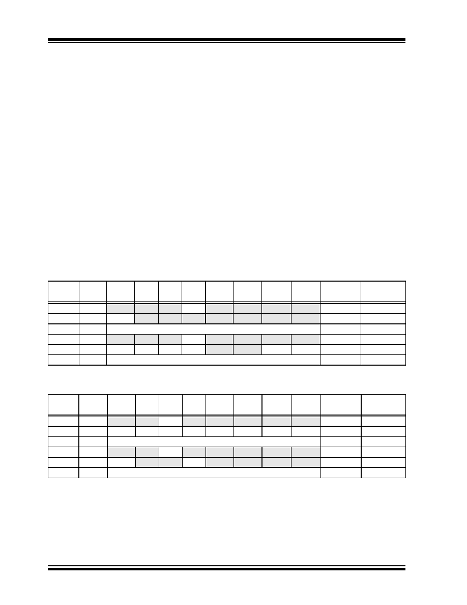
TABLE 12-11: REGISTERS ASSOCIATED WITH SYNCHRONOUS SLAVE TRANSMISSION
TABLE 12-12: REGISTERS ASSOCIATED WITH SYNCHRONOUS SLAVE RECEPTION
Address
Name
Bit 7
Bit 6
Bit 5
Bit 4
Bit 3
Bit 2
Bit 1
Bit 0
Value on
POR
Value on all
other Resets
0Ch
PIR1
EEIF
CMIF
RCIF
TXIF
—
CCP1IF TMR2IF TMR1IF 0000 -000
0000 -000
18h
RCSTA
SPEN
RX9
SREN CREN
ADEN
FERR
OERR
RX9D
0000 000x
19h
TXREG USART Transmit Data Register
0000 0000
8Ch
PIE1
EEIE
CMIE
RCIE
TXIE
—
CCP1IE TMR2IE TMR1IE 0000 -000
0000 -000
98h
TXSTA
CSRC
TX9
TXEN SYNC
—
BRGH
TRMT
TX9D
0000 -010
99h
SPBRG Baud Rate Generator Register
0000 0000
Legend:
x
= unknown, - = unimplemented read as ‘0’. Shaded cells are not used for synchronous slave transmission.
Address
Name
Bit 7
Bit 6
Bit 5
Bit 4
Bit 3
Bit 2
Bit 1
Bit 0
Value on
POR
Value on all
other Resets
0Ch
PIR1
EEIF
CMIF
RCIF
TXIF
—
CCP1IF TMR2IF TMR1IF 0000 -000
0000 -000
18h
RCSTA
SPEN
RX9
SREN CREN
ADEN
FERR
OERR
RX9D
0000 000x
1Ah
RCREG USART Receive Data Register
0000 0000
8Ch
PIE1
EEIE
CMIE
RCIE
TXIE
—
CCP1IE TMR2IE TMR1IE 0000 -000
0000 -000
98h
TXSTA
CSRC
TX9
TXEN SYNC
—
BRGH
TRMT
TX9D
0000 -010
99h
SPBRG Baud Rate Generator Register
0000 0000
Legend:
x
= unknown, - = unimplemented read as ‘0’. Shaded cells are not used for synchronous slave reception.
相关PDF资料 |
PDF描述 |
|---|---|
| PIC16C621A-40/SO | IC MCU OTP 1KX14 COMP 18SOIC |
| PIC16LC620AT-04/SS | IC MCU OTP 512X14 COMP 20SSOP |
| PIC16LC620AT-04I/SS | IC MCU OTP 512X14 COMP 20SSOP |
| VI-243-IX-S | CONVERTER MOD DC/DC 24V 75W |
| VE-2TR-IX-S | CONVERTER MOD DC/DC 7.5V 75W |
相关代理商/技术参数 |
参数描述 |
|---|---|
| PIC16LF627AT-I/ML | 功能描述:8位微控制器 -MCU 1.75KB 224 RAM 16I/O Ind Temp QFN28 RoHS:否 制造商:Silicon Labs 核心:8051 处理器系列:C8051F39x 数据总线宽度:8 bit 最大时钟频率:50 MHz 程序存储器大小:16 KB 数据 RAM 大小:1 KB 片上 ADC:Yes 工作电源电压:1.8 V to 3.6 V 工作温度范围:- 40 C to + 105 C 封装 / 箱体:QFN-20 安装风格:SMD/SMT |
| PIC16LF627AT-I/SO | 功能描述:8位微控制器 -MCU 1.75KB 224 RAM 16I/O Ind Temp SOIC18 RoHS:否 制造商:Silicon Labs 核心:8051 处理器系列:C8051F39x 数据总线宽度:8 bit 最大时钟频率:50 MHz 程序存储器大小:16 KB 数据 RAM 大小:1 KB 片上 ADC:Yes 工作电源电压:1.8 V to 3.6 V 工作温度范围:- 40 C to + 105 C 封装 / 箱体:QFN-20 安装风格:SMD/SMT |
| PIC16LF627AT-I/SS | 功能描述:8位微控制器 -MCU 1.75KB 224 RAM 16I/O Ind Temp SSOP20 RoHS:否 制造商:Silicon Labs 核心:8051 处理器系列:C8051F39x 数据总线宽度:8 bit 最大时钟频率:50 MHz 程序存储器大小:16 KB 数据 RAM 大小:1 KB 片上 ADC:Yes 工作电源电压:1.8 V to 3.6 V 工作温度范围:- 40 C to + 105 C 封装 / 箱体:QFN-20 安装风格:SMD/SMT |
| PIC16LF627-I/SS | 制造商:Microchip Technology Inc 功能描述: |
| PIC16LF627T-04/SO | 功能描述:8位微控制器 -MCU 1.75KB 224 RAM 16I/O 4MHz SOIC18 RoHS:否 制造商:Silicon Labs 核心:8051 处理器系列:C8051F39x 数据总线宽度:8 bit 最大时钟频率:50 MHz 程序存储器大小:16 KB 数据 RAM 大小:1 KB 片上 ADC:Yes 工作电源电压:1.8 V to 3.6 V 工作温度范围:- 40 C to + 105 C 封装 / 箱体:QFN-20 安装风格:SMD/SMT |
发布紧急采购,3分钟左右您将得到回复。