- 您现在的位置:买卖IC网 > PDF目录11560 > PIC16LF627A-I/ML (Microchip Technology)IC MCU FLASH 1KX14 EEPROM 28QFN PDF资料下载
参数资料
| 型号: | PIC16LF627A-I/ML |
| 厂商: | Microchip Technology |
| 文件页数: | 122/180页 |
| 文件大小: | 0K |
| 描述: | IC MCU FLASH 1KX14 EEPROM 28QFN |
| 产品培训模块: | Asynchronous Stimulus |
| 标准包装: | 61 |
| 系列: | PIC® 16F |
| 核心处理器: | PIC |
| 芯体尺寸: | 8-位 |
| 速度: | 20MHz |
| 连通性: | UART/USART |
| 外围设备: | 欠压检测/复位,POR,PWM,WDT |
| 输入/输出数: | 16 |
| 程序存储器容量: | 1.75KB(1K x 14) |
| 程序存储器类型: | 闪存 |
| EEPROM 大小: | 128 x 8 |
| RAM 容量: | 224 x 8 |
| 电压 - 电源 (Vcc/Vdd): | 2 V ~ 5.5 V |
| 振荡器型: | 内部 |
| 工作温度: | -40°C ~ 85°C |
| 封装/外壳: | 28-VQFN 裸露焊盘 |
| 包装: | 管件 |
第1页第2页第3页第4页第5页第6页第7页第8页第9页第10页第11页第12页第13页第14页第15页第16页第17页第18页第19页第20页第21页第22页第23页第24页第25页第26页第27页第28页第29页第30页第31页第32页第33页第34页第35页第36页第37页第38页第39页第40页第41页第42页第43页第44页第45页第46页第47页第48页第49页第50页第51页第52页第53页第54页第55页第56页第57页第58页第59页第60页第61页第62页第63页第64页第65页第66页第67页第68页第69页第70页第71页第72页第73页第74页第75页第76页第77页第78页第79页第80页第81页第82页第83页第84页第85页第86页第87页第88页第89页第90页第91页第92页第93页第94页第95页第96页第97页第98页第99页第100页第101页第102页第103页第104页第105页第106页第107页第108页第109页第110页第111页第112页第113页第114页第115页第116页第117页第118页第119页第120页第121页当前第122页第123页第124页第125页第126页第127页第128页第129页第130页第131页第132页第133页第134页第135页第136页第137页第138页第139页第140页第141页第142页第143页第144页第145页第146页第147页第148页第149页第150页第151页第152页第153页第154页第155页第156页第157页第158页第159页第160页第161页第162页第163页第164页第165页第166页第167页第168页第169页第170页第171页第172页第173页第174页第175页第176页第177页第178页第179页第180页
PIC16F627A/628A/648A
DS40044G-page 46
2009 Microchip Technology Inc.
5.3
I/O Programming Considerations
5.3.1
BIDIRECTIONAL I/O PORTS
Any instruction that writes operates internally as a read
followed by a write operation. The BCF and BSF
instructions, for example, read the register into the
CPU, execute the bit operation and write the result
back to the register. Caution must be used when these
instructions are applied to a port with both inputs and
outputs defined. For example, a BSF operation on bit 5
of PORTB will cause all eight bits of PORTB to be read
into the CPU. Then the BSF operation takes place on
bit 5 and PORTB is written to the output latches. If
another bit of PORTB is used as a bidirectional I/O pin
(e.g., bit 0) and is defined as an input at this time, the
input signal present on the pin itself would be read into
the CPU and rewritten to the data latch of this particular
pin, overwriting the previous content. As long as the pin
stays in the Input mode, no problem occurs. However,
if bit 0 is switched into Output mode later on, the
content of the data latch may now be unknown.
Reading a port register reads the values of the port
pins. Writing to the port register writes the value to the
port latch. When using read-modify-write instructions
(ex. BCF, BSF, etc.) on a port, the value of the port pins
is read, the desired operation is done to this value, and
this value is then written to the port latch.
Example 5-2 shows the effect of two sequential read-
modify-write instructions (ex., BCF, BSF, etc.) on an
I/O port.
A pin actively outputting a Low or High should not be
driven from external devices at the same time in order
to change the level on this pin (“wired-OR”, “wired-
AND”). The resulting high output currents may damage
the chip.
EXAMPLE 5-2:
READ-MODIFY-WRITE
INSTRUCTIONS ON AN
I/O PORT
5.3.2
SUCCESSIVE OPERATIONS ON I/O
PORTS
The actual write to an I/O port happens at the end of
an instruction cycle, whereas for reading, the data
must be valid at the beginning of the instruction cycle
(Figure 5-16). Therefore, care must be exercised if a
write followed by a read operation is carried out on the
same I/O port. The sequence of instructions should be
such to allow the pin voltage to stabilize (load
dependent) before the next instruction, which causes
that file to be read into the CPU, is executed. Other-
wise, the previous state of that pin may be read into
the CPU rather than the new state. When in doubt, it
is better to separate these instructions with a NOP or
another instruction not accessing this I/O port.
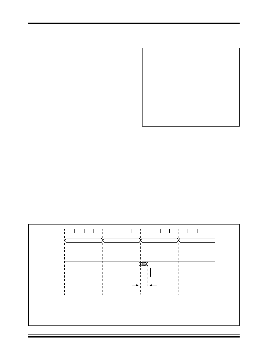
FIGURE 5-16:
SUCCESSIVE I/O OPERATION
;Initial PORT settings:PORTB<7:4> Inputs
;
PORTB<3:0> Outputs
;PORTB<7:6> have external pull-up and are
;not connected to other circuitry
;
PORT latchPORT Pins
---------- ----------
BCF STATUS, RP0
;
BCF PORTB, 7
;01pp pppp 11pp pppp
BSF STATUS, RP0
;
BCF TRISB, 7
;10pp pppp 11pp pppp
BCF TRISB, 6
;10pp pppp 10pp pppp
;
;Note that the user may have expected the
;pin values to be 00pp pppp. The 2nd BCF
;caused RB7 to be latched as the pin value
;(High).
Q1 Q2 Q3 Q4
PC
Instruction
fetched
Q1 Q2 Q3 Q4
Q1 Q2 Q3 Q4 Q1 Q2 Q3 Q4
PC + 1
PC
PC + 2
PC + 3
MOVWF
PORTB
Write to PORTB
MOVF
PORTB, W
Read to PORTB
NOP
TPD
Execute
MOVWF
PORTB
Execute
MOVF
PORTB, W
Port pin
sampled here
Execute
NOP
Note 1:
This example shows write to PORTB followed by a read from PORTB.
2:
Data setup time = (0.25 TCY - TPD) where TCY = instruction cycle and TPD = propagation delay of Q1 cycle
to output valid. Therefore, at higher clock frequencies, a write followed by a read may be problematic.
相关PDF资料 |
PDF描述 |
|---|---|
| PIC16C621A-40/SO | IC MCU OTP 1KX14 COMP 18SOIC |
| PIC16LC620AT-04/SS | IC MCU OTP 512X14 COMP 20SSOP |
| PIC16LC620AT-04I/SS | IC MCU OTP 512X14 COMP 20SSOP |
| VI-243-IX-S | CONVERTER MOD DC/DC 24V 75W |
| VE-2TR-IX-S | CONVERTER MOD DC/DC 7.5V 75W |
相关代理商/技术参数 |
参数描述 |
|---|---|
| PIC16LF627AT-I/ML | 功能描述:8位微控制器 -MCU 1.75KB 224 RAM 16I/O Ind Temp QFN28 RoHS:否 制造商:Silicon Labs 核心:8051 处理器系列:C8051F39x 数据总线宽度:8 bit 最大时钟频率:50 MHz 程序存储器大小:16 KB 数据 RAM 大小:1 KB 片上 ADC:Yes 工作电源电压:1.8 V to 3.6 V 工作温度范围:- 40 C to + 105 C 封装 / 箱体:QFN-20 安装风格:SMD/SMT |
| PIC16LF627AT-I/SO | 功能描述:8位微控制器 -MCU 1.75KB 224 RAM 16I/O Ind Temp SOIC18 RoHS:否 制造商:Silicon Labs 核心:8051 处理器系列:C8051F39x 数据总线宽度:8 bit 最大时钟频率:50 MHz 程序存储器大小:16 KB 数据 RAM 大小:1 KB 片上 ADC:Yes 工作电源电压:1.8 V to 3.6 V 工作温度范围:- 40 C to + 105 C 封装 / 箱体:QFN-20 安装风格:SMD/SMT |
| PIC16LF627AT-I/SS | 功能描述:8位微控制器 -MCU 1.75KB 224 RAM 16I/O Ind Temp SSOP20 RoHS:否 制造商:Silicon Labs 核心:8051 处理器系列:C8051F39x 数据总线宽度:8 bit 最大时钟频率:50 MHz 程序存储器大小:16 KB 数据 RAM 大小:1 KB 片上 ADC:Yes 工作电源电压:1.8 V to 3.6 V 工作温度范围:- 40 C to + 105 C 封装 / 箱体:QFN-20 安装风格:SMD/SMT |
| PIC16LF627-I/SS | 制造商:Microchip Technology Inc 功能描述: |
| PIC16LF627T-04/SO | 功能描述:8位微控制器 -MCU 1.75KB 224 RAM 16I/O 4MHz SOIC18 RoHS:否 制造商:Silicon Labs 核心:8051 处理器系列:C8051F39x 数据总线宽度:8 bit 最大时钟频率:50 MHz 程序存储器大小:16 KB 数据 RAM 大小:1 KB 片上 ADC:Yes 工作电源电压:1.8 V to 3.6 V 工作温度范围:- 40 C to + 105 C 封装 / 箱体:QFN-20 安装风格:SMD/SMT |
发布紧急采购,3分钟左右您将得到回复。