- 您现在的位置:买卖IC网 > PDF目录11489 > PIC18F2321-E/SS (Microchip Technology)IC PIC MCU FLASH 4KX16 28SSOP PDF资料下载
参数资料
| 型号: | PIC18F2321-E/SS |
| 厂商: | Microchip Technology |
| 文件页数: | 37/110页 |
| 文件大小: | 0K |
| 描述: | IC PIC MCU FLASH 4KX16 28SSOP |
| 产品培训模块: | Asynchronous Stimulus |
| 标准包装: | 47 |
| 系列: | PIC® 18F |
| 核心处理器: | PIC |
| 芯体尺寸: | 8-位 |
| 速度: | 25MHz |
| 连通性: | I²C,SPI,UART/USART |
| 外围设备: | 欠压检测/复位,HLVD,POR,PWM,WDT |
| 输入/输出数: | 25 |
| 程序存储器容量: | 8KB(4K x 16) |
| 程序存储器类型: | 闪存 |
| EEPROM 大小: | 256 x 8 |
| RAM 容量: | 512 x 8 |
| 电压 - 电源 (Vcc/Vdd): | 4.2 V ~ 5.5 V |
| 数据转换器: | A/D 10x10b |
| 振荡器型: | 内部 |
| 工作温度: | -40°C ~ 125°C |
| 封装/外壳: | 28-SSOP(0.209",5.30mm 宽) |
| 包装: | 管件 |
第1页第2页第3页第4页第5页第6页第7页第8页第9页第10页第11页第12页第13页第14页第15页第16页第17页第18页第19页第20页第21页第22页第23页第24页第25页第26页第27页第28页第29页第30页第31页第32页第33页第34页第35页第36页当前第37页第38页第39页第40页第41页第42页第43页第44页第45页第46页第47页第48页第49页第50页第51页第52页第53页第54页第55页第56页第57页第58页第59页第60页第61页第62页第63页第64页第65页第66页第67页第68页第69页第70页第71页第72页第73页第74页第75页第76页第77页第78页第79页第80页第81页第82页第83页第84页第85页第86页第87页第88页第89页第90页第91页第92页第93页第94页第95页第96页第97页第98页第99页第100页第101页第102页第103页第104页第105页第106页第107页第108页第109页第110页
PIC18F2221/2321/4221/4321 FAMILY
DS39689F-page 32
2009 Microchip Technology Inc.
3.6
Internal Oscillator Block
The PIC18F2221/2321/4221/4321 family of devices
includes an internal oscillator block which generates
two different clock signals; either can be used as the
microcontroller’s clock source. This may eliminate the
need for external oscillator circuits on the OSC1 and/or
OSC2 pins.
The main output (INTOSC) is an 8 MHz clock source,
which can be used to directly drive the device clock. It
also drives a postscaler, which can provide a range of
clock frequencies from 31 kHz to 4 MHz. The INTOSC
output is enabled when a clock frequency from 125 kHz
to 8 MHz is selected. The INTOSC output can also be
enabled when 31 kHz is selected, depending on the
INTSRC bit (OSCTUNE<7>).
The other clock source is the internal RC oscillator
(INTRC), which provides a nominal 31 kHz output.
INTRC is enabled if it is selected as the device clock
source; it is also enabled automatically when any of the
following are enabled:
Power-up Timer
Fail-Safe Clock Monitor
Watchdog Timer
Two-Speed Start-up
These features are discussed in greater detail in
The clock source frequency (INTOSC direct, INTRC
direct or INTOSC postscaler) is selected by configuring
the IRCF bits of the OSCCON register (page 37).
3.6.1
INTIO MODES
Using the internal oscillator as the clock source elimi-
nates the need for up to two external oscillator pins,
which can then be used for digital I/O. Two distinct
configurations are available:
In INTIO1 mode, the OSC2 pin outputs FOSC/4,
while OSC1 functions as RA7 (see Figure 3-8) for
digital input and output.
In INTIO2 mode, OSC1 functions as RA7 and
OSC2 functions as RA6 (see Figure 3-9), both for
digital input and output.
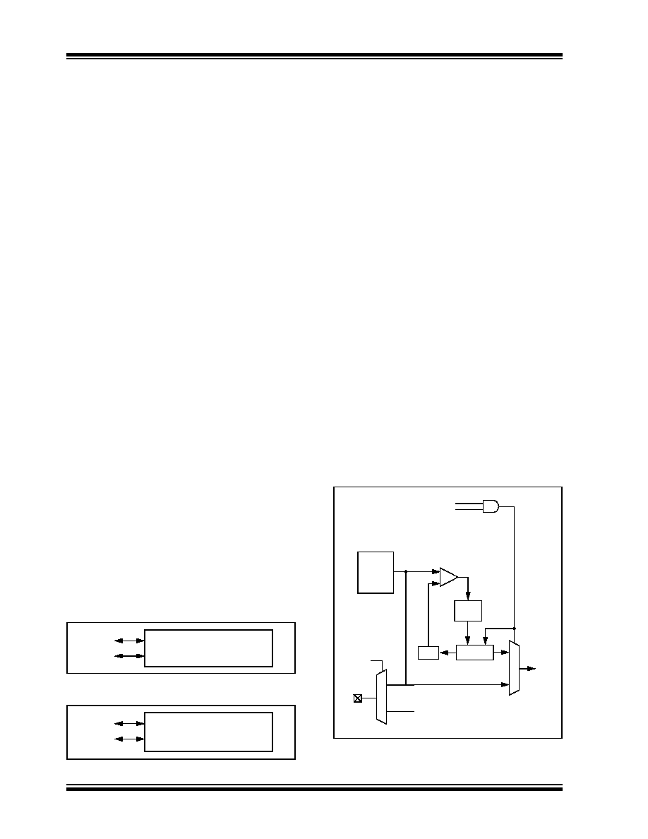
FIGURE 3-8:
INTIO1 OSCILLATOR MODE
FIGURE 3-9:
INTIO2 OSCILLATOR MODE
3.6.2
INTOSC OUTPUT FREQUENCY
The internal oscillator block is calibrated at the factory
to produce an INTOSC output frequency of 8 MHz.
The INTRC oscillator operates independently of the
INTOSC source. Any changes in INTOSC across
voltage and temperature are not necessarily reflected
by changes in INTRC or vice versa.
3.6.3
OSCTUNE REGISTER
The INTOSC output has been calibrated at the
factory but can be adjusted in the user’s application.
This
is
done
by
writing
to
TUN<4:0>
(OSCTUNE<4:0>)
in
the
OSCTUNE
register
When the OSCTUNE register is modified, the INTOSC
frequency will begin shifting to the new frequency.
Code execution continues during this shift. There is no
indication that the shift has occurred. The INTRC is not
affected by OSCTUNE.
The OSCTUNE register also implements the INTSRC
(OSCTUNE<7>) and PLLEN (OSCTUNE<6>) bits,
which control certain features of the internal oscillator
block. The INTSRC bit allows users to select which
internal oscillator provides the clock source when the
31 kHz frequency option is selected. This is covered in
greater detail in Section 3.7.1 “Oscillator Control
The PLLEN bit controls the operation of the Phase
Locked Loop (PLL) in Internal Oscillator modes (see
FIGURE 3-10:
INTOSC AND PLL BLOCK
DIAGRAM
PIC18FXXXX
OSC2
FOSC/4
I/O (OSC1)
RA7
PIC18FXXXX
I/O (OSC2)
RA6
I/O (OSC1)
RA7
MU
X
VCO
Loop
Filter
OSC2
PLLEN
FIN
FOUT
SYSCLK
Phase
Comparator
8 or 4 MHz
÷4
(OSCTUNE<6>)
MUX
RA6
CLKO
INTOSC
相关PDF资料 |
PDF描述 |
|---|---|
| PIC16LC771/SS | IC MCU OTP 4KX14 A/D PWM 20SSOP |
| ADG211AKRZ | IC SWITCH QUAD SPST 16SOIC |
| PIC16F88T-I/SO | IC MCU FLASH 4KX14 EEPROM 18SOIC |
| PIC16C710T-20I/SO | IC MCU OTP 512X14 A/D 18SOIC |
| VE-25F-IY-B1 | CONVERTER MOD DC/DC 72V 50W |
相关代理商/技术参数 |
参数描述 |
|---|---|
| PIC18F2321-I/ML | 功能描述:8位微控制器 -MCU 8 KB Flash 512 RAM RoHS:否 制造商:Silicon Labs 核心:8051 处理器系列:C8051F39x 数据总线宽度:8 bit 最大时钟频率:50 MHz 程序存储器大小:16 KB 数据 RAM 大小:1 KB 片上 ADC:Yes 工作电源电压:1.8 V to 3.6 V 工作温度范围:- 40 C to + 105 C 封装 / 箱体:QFN-20 安装风格:SMD/SMT |
| PIC18F2321-I/SO | 功能描述:8位微控制器 -MCU 8 KB Flash 512 RAM RoHS:否 制造商:Silicon Labs 核心:8051 处理器系列:C8051F39x 数据总线宽度:8 bit 最大时钟频率:50 MHz 程序存储器大小:16 KB 数据 RAM 大小:1 KB 片上 ADC:Yes 工作电源电压:1.8 V to 3.6 V 工作温度范围:- 40 C to + 105 C 封装 / 箱体:QFN-20 安装风格:SMD/SMT |
| PIC18F2321-I/SP | 功能描述:8位微控制器 -MCU 8 KB Flash 512 RAM RoHS:否 制造商:Silicon Labs 核心:8051 处理器系列:C8051F39x 数据总线宽度:8 bit 最大时钟频率:50 MHz 程序存储器大小:16 KB 数据 RAM 大小:1 KB 片上 ADC:Yes 工作电源电压:1.8 V to 3.6 V 工作温度范围:- 40 C to + 105 C 封装 / 箱体:QFN-20 安装风格:SMD/SMT |
| PIC18F2321-I/SP | 制造商:Microchip Technology Inc 功能描述:8-Bit Microcontroller IC |
| PIC18F2321-I/SS | 功能描述:8位微控制器 -MCU 8KB Flash 512bytes RoHS:否 制造商:Silicon Labs 核心:8051 处理器系列:C8051F39x 数据总线宽度:8 bit 最大时钟频率:50 MHz 程序存储器大小:16 KB 数据 RAM 大小:1 KB 片上 ADC:Yes 工作电源电压:1.8 V to 3.6 V 工作温度范围:- 40 C to + 105 C 封装 / 箱体:QFN-20 安装风格:SMD/SMT |
发布紧急采购,3分钟左右您将得到回复。