- 您现在的位置:买卖IC网 > PDF目录11491 > PIC18F2450T-I/SO (Microchip Technology)IC PIC MCU FLASH 8KX16 28SOIC PDF资料下载
参数资料
| 型号: | PIC18F2450T-I/SO |
| 厂商: | Microchip Technology |
| 文件页数: | 123/241页 |
| 文件大小: | 0K |
| 描述: | IC PIC MCU FLASH 8KX16 28SOIC |
| 产品培训模块: | Asynchronous Stimulus |
| 标准包装: | 1,600 |
| 系列: | PIC® 18F |
| 核心处理器: | PIC |
| 芯体尺寸: | 8-位 |
| 速度: | 48MHz |
| 连通性: | UART/USART,USB |
| 外围设备: | 欠压检测/复位,HLVD,POR,PWM,WDT |
| 输入/输出数: | 23 |
| 程序存储器容量: | 16KB(8K x 16) |
| 程序存储器类型: | 闪存 |
| RAM 容量: | 768 x 8 |
| 电压 - 电源 (Vcc/Vdd): | 4.2 V ~ 5.5 V |
| 数据转换器: | A/D 10x10b |
| 振荡器型: | 内部 |
| 工作温度: | -40°C ~ 85°C |
| 封装/外壳: | 28-SOIC(0.295",7.50mm 宽) |
| 包装: | 带卷 (TR) |
| 配用: | DM163025-ND - PIC DEM FULL SPEED USB DEMO BRD |
第1页第2页第3页第4页第5页第6页第7页第8页第9页第10页第11页第12页第13页第14页第15页第16页第17页第18页第19页第20页第21页第22页第23页第24页第25页第26页第27页第28页第29页第30页第31页第32页第33页第34页第35页第36页第37页第38页第39页第40页第41页第42页第43页第44页第45页第46页第47页第48页第49页第50页第51页第52页第53页第54页第55页第56页第57页第58页第59页第60页第61页第62页第63页第64页第65页第66页第67页第68页第69页第70页第71页第72页第73页第74页第75页第76页第77页第78页第79页第80页第81页第82页第83页第84页第85页第86页第87页第88页第89页第90页第91页第92页第93页第94页第95页第96页第97页第98页第99页第100页第101页第102页第103页第104页第105页第106页第107页第108页第109页第110页第111页第112页第113页第114页第115页第116页第117页第118页第119页第120页第121页第122页当前第123页第124页第125页第126页第127页第128页第129页第130页第131页第132页第133页第134页第135页第136页第137页第138页第139页第140页第141页第142页第143页第144页第145页第146页第147页第148页第149页第150页第151页第152页第153页第154页第155页第156页第157页第158页第159页第160页第161页第162页第163页第164页第165页第166页第167页第168页第169页第170页第171页第172页第173页第174页第175页第176页第177页第178页第179页第180页第181页第182页第183页第184页第185页第186页第187页第188页第189页第190页第191页第192页第193页第194页第195页第196页第197页第198页第199页第200页第201页第202页第203页第204页第205页第206页第207页第208页第209页第210页第211页第212页第213页第214页第215页第216页第217页第218页第219页第220页第221页第222页第223页第224页第225页第226页第227页第228页第229页第230页第231页第232页第233页第234页第235页第236页第237页第238页第239页第240页第241页
209
XMEGA A [MANUAL]
8077I–AVR–11/2012
A high-to-low transition on the SCL line will force the line low for all masters on the bus, and they will start timing their low
clock period. The timing length of the low clock period can vary among the masters. When a master (DEVICE1 in this
case) has completed its low period, it releases the SCL line. However, the SCL line will not go high until all masters have
released it. Consequently, the SCL line will be held low by the device with the longest low period (DEVICE2). Devices
with shorter low periods must insert a wait state until the clock is released. All masters start their high period when the
SCL line is released by all devices and has gone high. The device which first completes its high period (DEVICE1) forces
the clock line low, and the procedure is then repeated. The result is that the device with the shortest clock period
determines the high period, while the low period of the clock is determined by the device with the longest clock period.
19.4
TWI Bus State Logic
The bus state logic continuously monitors the activity on the TWI bus lines when the master is enabled. It continues to
operate in all sleep modes, including power-down.
The bus state logic includes START and STOP condition detectors, collision detection, inactive bus timeout detection,
and a bit counter. Theseare used to determine the bus state. Software can get the current bus state by reading the bus
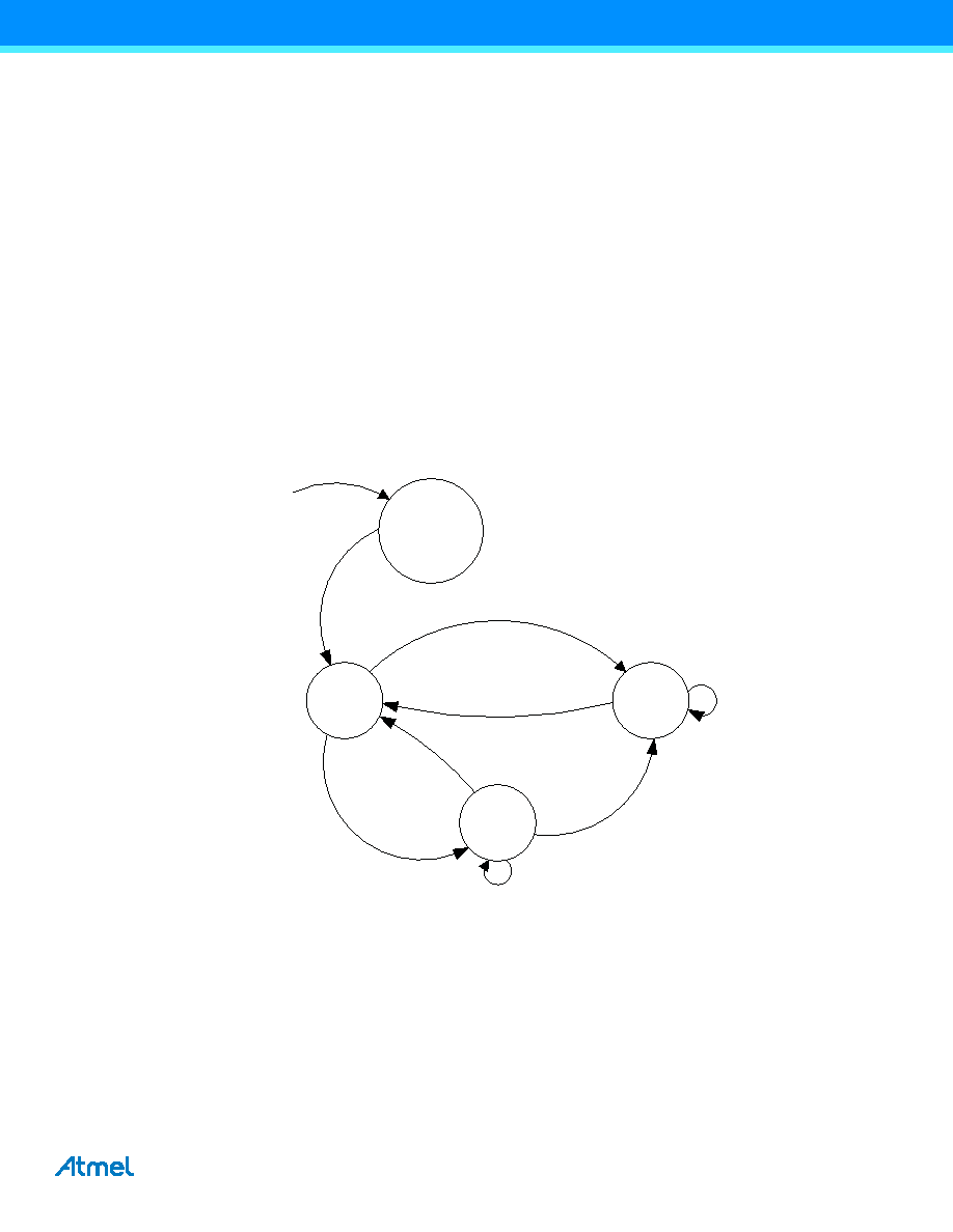
state bits in the master status register. The bus state can be unknown, idle, busy, or owner, and is determined according
to the state diagram shown in Figure 19-11. The values of the bus state bits according to state are shown in binary in the
figure.
Figure 19-11.Bus state, state diagram.
After a system reset and/or TWI master enable, the bus state is unknown. The bus state machine can be forced to enter
idle by writing to the bus state bits accordingly. If no state is set by application software, the bus state will become idle
when the first STOP condition is detected. If the master inactive bus timeout is enabled, the bus state will change to idle
on the occurrence of a timeout. After a known bus state is established, only a system reset or disabling of the TWI master
will set the state to unknown.
When the bus is idle, it is ready for a new transaction. If a START condition generated externally is detected, the bus
becomes busy until a STOP condition is detected. The STOP condition will change the bus state to idle. If the master
inactive bus timeout is enabled, the bus state will change from busy to idle on the occurrence of a timeout.
If a START condition is generated internally while in idle state, the owner state is entered. If the complete transaction was
performed without interference, i.e., no collisions are detected, the master will issue a STOP condition and the bus state
P + Timeout
Write ADDRESS
IDLE
(0b01)
S
BUSY
(0b11)
UNKNOWN
(0b00)
OWNER
(0b10)
Arbitration
Lost
Command P
Write
ADDRESS(Sr)
Sr
(S)
RESET
P + Timeout
相关PDF资料 |
PDF描述 |
|---|---|
| PIC24FJ32GA102T-I/SO | IC MCU 16BIT 32KB FLASH 28SOIC |
| PIC16CE624-20/SS | IC MCU OTP 1KX14 EE COMP 20SSOP |
| VI-2WV-IY-B1 | CONVERTER MOD DC/DC 5.8V 50W |
| PIC16CE624-20I/P | IC MCU OTP 1KX14 EE COMP 18DIP |
| VI-21P-IY-B1 | CONVERTER MOD DC/DC 13.8V 50W |
相关代理商/技术参数 |
参数描述 |
|---|---|
| PIC18F2455-I/SO | 功能描述:8位微控制器 -MCU 24kBF 2048RM FSUSB2 RoHS:否 制造商:Silicon Labs 核心:8051 处理器系列:C8051F39x 数据总线宽度:8 bit 最大时钟频率:50 MHz 程序存储器大小:16 KB 数据 RAM 大小:1 KB 片上 ADC:Yes 工作电源电压:1.8 V to 3.6 V 工作温度范围:- 40 C to + 105 C 封装 / 箱体:QFN-20 安装风格:SMD/SMT |
| PIC18F2455-I/SO | 制造商:Microchip Technology Inc 功能描述:IC 8BIT FLASH MCU 18F2455 SOIC28 |
| PIC18F2455-I/SP | 功能描述:8位微控制器 -MCU 24kBF 2048RM FSUSB2 RoHS:否 制造商:Silicon Labs 核心:8051 处理器系列:C8051F39x 数据总线宽度:8 bit 最大时钟频率:50 MHz 程序存储器大小:16 KB 数据 RAM 大小:1 KB 片上 ADC:Yes 工作电源电压:1.8 V to 3.6 V 工作温度范围:- 40 C to + 105 C 封装 / 箱体:QFN-20 安装风格:SMD/SMT |
| PIC18F2455-I/SP | 制造商:Microchip Technology Inc 功能描述:8-Bit Microcontroller IC |
| PIC18F2455T-I/SO | 功能描述:8位微控制器 -MCU 24kBF 2048RM FSUSB2 RoHS:否 制造商:Silicon Labs 核心:8051 处理器系列:C8051F39x 数据总线宽度:8 bit 最大时钟频率:50 MHz 程序存储器大小:16 KB 数据 RAM 大小:1 KB 片上 ADC:Yes 工作电源电压:1.8 V to 3.6 V 工作温度范围:- 40 C to + 105 C 封装 / 箱体:QFN-20 安装风格:SMD/SMT |
发布紧急采购,3分钟左右您将得到回复。