- 您现在的位置:买卖IC网 > PDF目录11491 > PIC18F2450T-I/SO (Microchip Technology)IC PIC MCU FLASH 8KX16 28SOIC PDF资料下载
参数资料
| 型号: | PIC18F2450T-I/SO |
| 厂商: | Microchip Technology |
| 文件页数: | 141/241页 |
| 文件大小: | 0K |
| 描述: | IC PIC MCU FLASH 8KX16 28SOIC |
| 产品培训模块: | Asynchronous Stimulus |
| 标准包装: | 1,600 |
| 系列: | PIC® 18F |
| 核心处理器: | PIC |
| 芯体尺寸: | 8-位 |
| 速度: | 48MHz |
| 连通性: | UART/USART,USB |
| 外围设备: | 欠压检测/复位,HLVD,POR,PWM,WDT |
| 输入/输出数: | 23 |
| 程序存储器容量: | 16KB(8K x 16) |
| 程序存储器类型: | 闪存 |
| RAM 容量: | 768 x 8 |
| 电压 - 电源 (Vcc/Vdd): | 4.2 V ~ 5.5 V |
| 数据转换器: | A/D 10x10b |
| 振荡器型: | 内部 |
| 工作温度: | -40°C ~ 85°C |
| 封装/外壳: | 28-SOIC(0.295",7.50mm 宽) |
| 包装: | 带卷 (TR) |
| 配用: | DM163025-ND - PIC DEM FULL SPEED USB DEMO BRD |
第1页第2页第3页第4页第5页第6页第7页第8页第9页第10页第11页第12页第13页第14页第15页第16页第17页第18页第19页第20页第21页第22页第23页第24页第25页第26页第27页第28页第29页第30页第31页第32页第33页第34页第35页第36页第37页第38页第39页第40页第41页第42页第43页第44页第45页第46页第47页第48页第49页第50页第51页第52页第53页第54页第55页第56页第57页第58页第59页第60页第61页第62页第63页第64页第65页第66页第67页第68页第69页第70页第71页第72页第73页第74页第75页第76页第77页第78页第79页第80页第81页第82页第83页第84页第85页第86页第87页第88页第89页第90页第91页第92页第93页第94页第95页第96页第97页第98页第99页第100页第101页第102页第103页第104页第105页第106页第107页第108页第109页第110页第111页第112页第113页第114页第115页第116页第117页第118页第119页第120页第121页第122页第123页第124页第125页第126页第127页第128页第129页第130页第131页第132页第133页第134页第135页第136页第137页第138页第139页第140页当前第141页第142页第143页第144页第145页第146页第147页第148页第149页第150页第151页第152页第153页第154页第155页第156页第157页第158页第159页第160页第161页第162页第163页第164页第165页第166页第167页第168页第169页第170页第171页第172页第173页第174页第175页第176页第177页第178页第179页第180页第181页第182页第183页第184页第185页第186页第187页第188页第189页第190页第191页第192页第193页第194页第195页第196页第197页第198页第199页第200页第201页第202页第203页第204页第205页第206页第207页第208页第209页第210页第211页第212页第213页第214页第215页第216页第217页第218页第219页第220页第221页第222页第223页第224页第225页第226页第227页第228页第229页第230页第231页第232页第233页第234页第235页第236页第237页第238页第239页第240页第241页
225
XMEGA A [MANUAL]
8077I–AVR–11/2012
20.
SPI – Serial Peripheral Interface
20.1
Features
Full-duplex, three-wire synchronous data transfer
Master or slave operation
Lsb first or msb first data transfer
Eight programmable bit rates
Interrupt flag at the end of transmission
Write collision flag to indicate data collision
Wake up from idle sleep mode
Double speed master mode
20.2
Overview
The Serial Peripheral Interface (SPI) is a high-speed synchronous data transfer interface using three or four pins. It
allows fast communication between an XMEGA device and peripheral devices or between several microcontrollers. The
SPI supports full-duplex communication.
A device connected to the bus must act as a master or slave.The master initiates and controls all data transactions. The
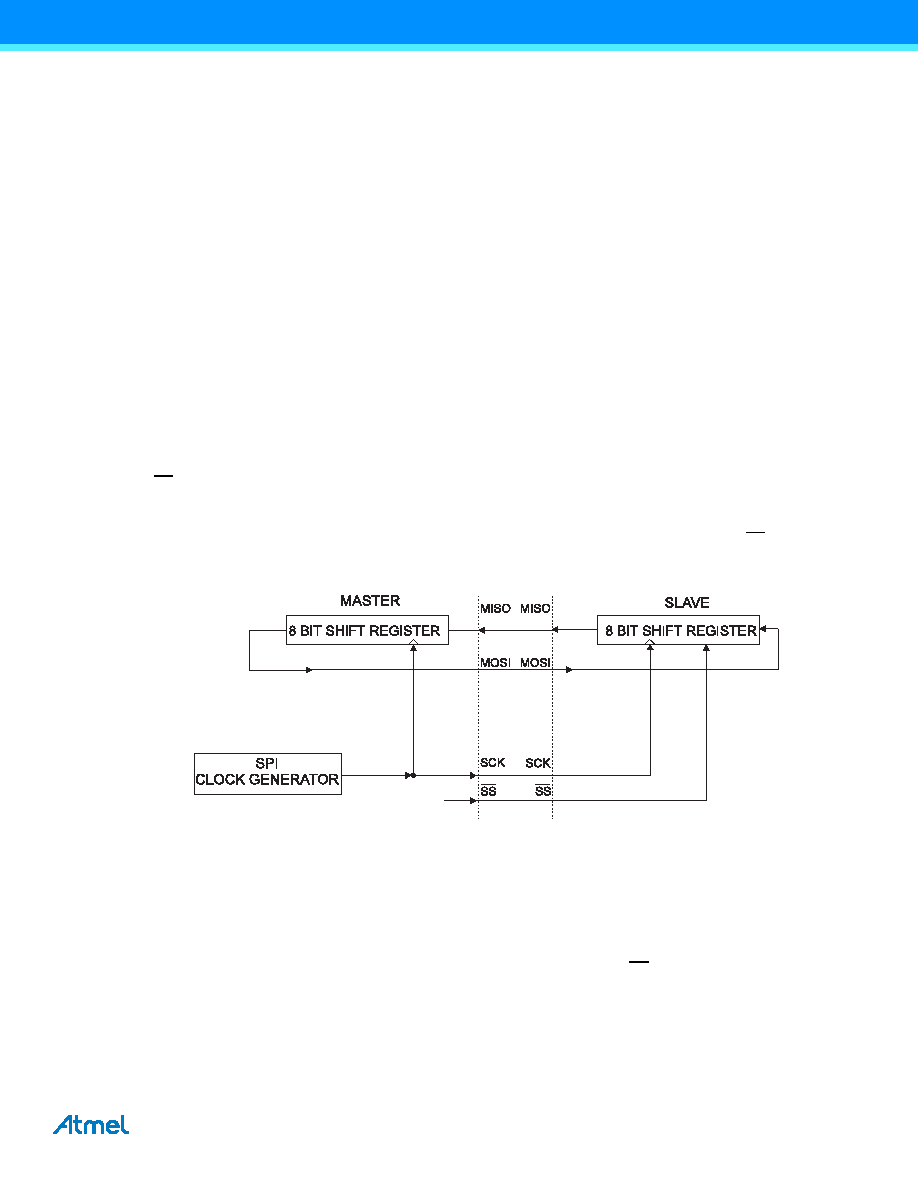
interconnection between master and slave devices with SPI is shown in Figure 20-1 on page 225. The system consists of
two shift registers and a master clock generator. The SPI master initiates the communication cycle by pulling the slave
select (SS) signal low for the desired slave. Master and slave prepare the data to be sent in their respective shift
registers, and the master generates the required clock pulses on the SCK line to interchange data. Data are always
shifted from master to slave on the master output, slave input (MOSI) line, and from slave to master on the master input,
slave output (MISO) line. After each data packet, the master can synchronize the slave by pulling the SS line high.
Figure 20-1. SPI master-slave interconnection.
The SPI module is unbuffered in the transmit direction and single buffered in the receive direction. This means that bytes
to be transmitted cannot be written to the SPI DATA register before the entire shift cycle is completed. When receiving
data, a received character must be read from the DATA register before the next character has been completely shifted in.
Otherwise, the first byte will be lost.
In SPI slave mode, the control logic will sample the incoming signal on the SCK pin. To ensure correct sampling of this
clock signal, the minimum low and high periods must each be longer than two CPU clock cycles.
When the SPI module is enabled, the data direction of the MOSI, MISO, SCK, and SS pins is overridden according to
Table 20-1 on page 226. The pins with user-defined direction must be configured from software to have the correct
direction according to the application.
SHIFT
ENABLE
msb
lsb
msb
lsb
相关PDF资料 |
PDF描述 |
|---|---|
| PIC24FJ32GA102T-I/SO | IC MCU 16BIT 32KB FLASH 28SOIC |
| PIC16CE624-20/SS | IC MCU OTP 1KX14 EE COMP 20SSOP |
| VI-2WV-IY-B1 | CONVERTER MOD DC/DC 5.8V 50W |
| PIC16CE624-20I/P | IC MCU OTP 1KX14 EE COMP 18DIP |
| VI-21P-IY-B1 | CONVERTER MOD DC/DC 13.8V 50W |
相关代理商/技术参数 |
参数描述 |
|---|---|
| PIC18F2455-I/SO | 功能描述:8位微控制器 -MCU 24kBF 2048RM FSUSB2 RoHS:否 制造商:Silicon Labs 核心:8051 处理器系列:C8051F39x 数据总线宽度:8 bit 最大时钟频率:50 MHz 程序存储器大小:16 KB 数据 RAM 大小:1 KB 片上 ADC:Yes 工作电源电压:1.8 V to 3.6 V 工作温度范围:- 40 C to + 105 C 封装 / 箱体:QFN-20 安装风格:SMD/SMT |
| PIC18F2455-I/SO | 制造商:Microchip Technology Inc 功能描述:IC 8BIT FLASH MCU 18F2455 SOIC28 |
| PIC18F2455-I/SP | 功能描述:8位微控制器 -MCU 24kBF 2048RM FSUSB2 RoHS:否 制造商:Silicon Labs 核心:8051 处理器系列:C8051F39x 数据总线宽度:8 bit 最大时钟频率:50 MHz 程序存储器大小:16 KB 数据 RAM 大小:1 KB 片上 ADC:Yes 工作电源电压:1.8 V to 3.6 V 工作温度范围:- 40 C to + 105 C 封装 / 箱体:QFN-20 安装风格:SMD/SMT |
| PIC18F2455-I/SP | 制造商:Microchip Technology Inc 功能描述:8-Bit Microcontroller IC |
| PIC18F2455T-I/SO | 功能描述:8位微控制器 -MCU 24kBF 2048RM FSUSB2 RoHS:否 制造商:Silicon Labs 核心:8051 处理器系列:C8051F39x 数据总线宽度:8 bit 最大时钟频率:50 MHz 程序存储器大小:16 KB 数据 RAM 大小:1 KB 片上 ADC:Yes 工作电源电压:1.8 V to 3.6 V 工作温度范围:- 40 C to + 105 C 封装 / 箱体:QFN-20 安装风格:SMD/SMT |
发布紧急采购,3分钟左右您将得到回复。