- 您现在的位置:买卖IC网 > PDF目录11491 > PIC18F2450T-I/SO (Microchip Technology)IC PIC MCU FLASH 8KX16 28SOIC PDF资料下载
参数资料
| 型号: | PIC18F2450T-I/SO |
| 厂商: | Microchip Technology |
| 文件页数: | 68/241页 |
| 文件大小: | 0K |
| 描述: | IC PIC MCU FLASH 8KX16 28SOIC |
| 产品培训模块: | Asynchronous Stimulus |
| 标准包装: | 1,600 |
| 系列: | PIC® 18F |
| 核心处理器: | PIC |
| 芯体尺寸: | 8-位 |
| 速度: | 48MHz |
| 连通性: | UART/USART,USB |
| 外围设备: | 欠压检测/复位,HLVD,POR,PWM,WDT |
| 输入/输出数: | 23 |
| 程序存储器容量: | 16KB(8K x 16) |
| 程序存储器类型: | 闪存 |
| RAM 容量: | 768 x 8 |
| 电压 - 电源 (Vcc/Vdd): | 4.2 V ~ 5.5 V |
| 数据转换器: | A/D 10x10b |
| 振荡器型: | 内部 |
| 工作温度: | -40°C ~ 85°C |
| 封装/外壳: | 28-SOIC(0.295",7.50mm 宽) |
| 包装: | 带卷 (TR) |
| 配用: | DM163025-ND - PIC DEM FULL SPEED USB DEMO BRD |
第1页第2页第3页第4页第5页第6页第7页第8页第9页第10页第11页第12页第13页第14页第15页第16页第17页第18页第19页第20页第21页第22页第23页第24页第25页第26页第27页第28页第29页第30页第31页第32页第33页第34页第35页第36页第37页第38页第39页第40页第41页第42页第43页第44页第45页第46页第47页第48页第49页第50页第51页第52页第53页第54页第55页第56页第57页第58页第59页第60页第61页第62页第63页第64页第65页第66页第67页当前第68页第69页第70页第71页第72页第73页第74页第75页第76页第77页第78页第79页第80页第81页第82页第83页第84页第85页第86页第87页第88页第89页第90页第91页第92页第93页第94页第95页第96页第97页第98页第99页第100页第101页第102页第103页第104页第105页第106页第107页第108页第109页第110页第111页第112页第113页第114页第115页第116页第117页第118页第119页第120页第121页第122页第123页第124页第125页第126页第127页第128页第129页第130页第131页第132页第133页第134页第135页第136页第137页第138页第139页第140页第141页第142页第143页第144页第145页第146页第147页第148页第149页第150页第151页第152页第153页第154页第155页第156页第157页第158页第159页第160页第161页第162页第163页第164页第165页第166页第167页第168页第169页第170页第171页第172页第173页第174页第175页第176页第177页第178页第179页第180页第181页第182页第183页第184页第185页第186页第187页第188页第189页第190页第191页第192页第193页第194页第195页第196页第197页第198页第199页第200页第201页第202页第203页第204页第205页第206页第207页第208页第209页第210页第211页第212页第213页第214页第215页第216页第217页第218页第219页第220页第221页第222页第223页第224页第225页第226页第227页第228页第229页第230页第231页第232页第233页第234页第235页第236页第237页第238页第239页第240页第241页
dsPIC30F3010/3011
DS70141F-page 16
2010 Microchip Technology Inc.
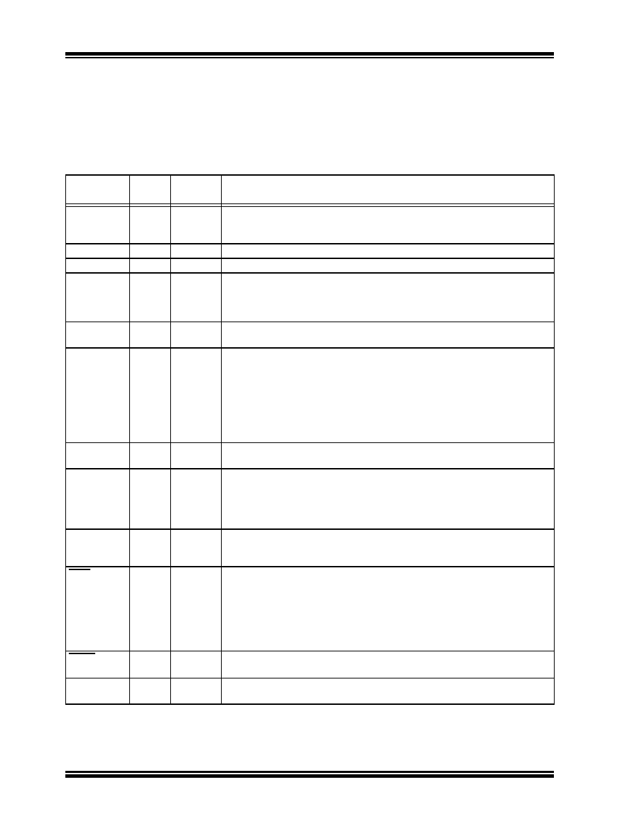
Table 1-2 provides a brief description of the device I/O
pinout and the functions that are multiplexed to a port
pin. Multiple functions may exist on one port pin. When
multiplexing occurs, the peripheral module’s functional
requirements may force an override of the data
direction of the port pin.
TABLE 1-2:
dsPIC30F3010 I/O PIN DESCRIPTIONS
Pin Name
Pin
Type
Buffer
Type
Description
AN0-AN5
I
Analog
Analog input channels.
AN0 and AN1 are also used for device programming data and clock inputs,
respectively.
AVDD
P
Positive supply for analog module. This pin must be connected at all times.
AVSS
P
Ground reference for analog module. This pin must be connected at all times.
CLKI
CLKO
I
O
ST/CMOS
—
External clock source input. Always associated with OSC1 pin function.
Oscillator crystal output. Connects to crystal or resonator in Crystal
Oscillator mode. Optionally functions as CLKO in RC and EC modes.
Always associated with OSC2 pin function.
CN0-CN7
I
ST
Input change notification inputs.
Can be software programmed for internal weak pull-ups on all inputs.
EMUD
EMUC
EMUD1
EMUC1
EMUD2
EMUC2
EMUD3
EMUC3
I/O
ST
ICD Primary Communication Channel data input/output pin.
ICD Primary Communication Channel clock input/output pin.
ICD Secondary Communication Channel data input/output pin.
ICD Secondary Communication Channel clock input/output pin.
ICD Tertiary Communication Channel data input/output pin.
ICD Tertiary Communication Channel clock input/output pin.
ICD Quaternary Communication Channel data input/output pin.
ICD Quaternary Communication Channel clock input/output pin.
IC1, IC2, IC7,
IC8
I
ST
Capture inputs 1, 2, 7 and 8.
INDX
QEA
QEB
I
ST
Quadrature Encoder Index Pulse input.
Quadrature Encoder Phase A input in QEI mode.
Auxiliary Timer External Clock/Gate input in Timer mode.
Quadrature Encoder Phase B input in QEI mode.
Auxiliary Timer External Clock/Gate input in Timer mode.
INT0
INT1
INT2
I
ST
External interrupt 0.
External interrupt 1.
External interrupt 2.
FLTA
PWM1L
PWM1H
PWM2L
PWM2H
PWM3L
PWM3H
I
O
ST
—
PWM Fault A input.
PWM1 Low output.
PWM1 High output.
PWM2 Low output.
PWM2 High output.
PWM3 Low output.
PWM3 High output.
MCLR
I/P
ST
Master Clear (Reset) input or programming voltage input. This pin is an active
low Reset to the device.
OCFA
OC1, OC2
I
O
ST
—
Compare Fault A input (for Compare channels 1, 2, 3 and 4).
Compare outputs 1 and 2.
Legend: CMOS =
CMOS compatible input or output
Analog =
Analog input
ST
=
Schmitt Trigger input with CMOS levels
O
=
Output
I
=
Input
P
=
Power
相关PDF资料 |
PDF描述 |
|---|---|
| PIC24FJ32GA102T-I/SO | IC MCU 16BIT 32KB FLASH 28SOIC |
| PIC16CE624-20/SS | IC MCU OTP 1KX14 EE COMP 20SSOP |
| VI-2WV-IY-B1 | CONVERTER MOD DC/DC 5.8V 50W |
| PIC16CE624-20I/P | IC MCU OTP 1KX14 EE COMP 18DIP |
| VI-21P-IY-B1 | CONVERTER MOD DC/DC 13.8V 50W |
相关代理商/技术参数 |
参数描述 |
|---|---|
| PIC18F2455-I/SO | 功能描述:8位微控制器 -MCU 24kBF 2048RM FSUSB2 RoHS:否 制造商:Silicon Labs 核心:8051 处理器系列:C8051F39x 数据总线宽度:8 bit 最大时钟频率:50 MHz 程序存储器大小:16 KB 数据 RAM 大小:1 KB 片上 ADC:Yes 工作电源电压:1.8 V to 3.6 V 工作温度范围:- 40 C to + 105 C 封装 / 箱体:QFN-20 安装风格:SMD/SMT |
| PIC18F2455-I/SO | 制造商:Microchip Technology Inc 功能描述:IC 8BIT FLASH MCU 18F2455 SOIC28 |
| PIC18F2455-I/SP | 功能描述:8位微控制器 -MCU 24kBF 2048RM FSUSB2 RoHS:否 制造商:Silicon Labs 核心:8051 处理器系列:C8051F39x 数据总线宽度:8 bit 最大时钟频率:50 MHz 程序存储器大小:16 KB 数据 RAM 大小:1 KB 片上 ADC:Yes 工作电源电压:1.8 V to 3.6 V 工作温度范围:- 40 C to + 105 C 封装 / 箱体:QFN-20 安装风格:SMD/SMT |
| PIC18F2455-I/SP | 制造商:Microchip Technology Inc 功能描述:8-Bit Microcontroller IC |
| PIC18F2455T-I/SO | 功能描述:8位微控制器 -MCU 24kBF 2048RM FSUSB2 RoHS:否 制造商:Silicon Labs 核心:8051 处理器系列:C8051F39x 数据总线宽度:8 bit 最大时钟频率:50 MHz 程序存储器大小:16 KB 数据 RAM 大小:1 KB 片上 ADC:Yes 工作电源电压:1.8 V to 3.6 V 工作温度范围:- 40 C to + 105 C 封装 / 箱体:QFN-20 安装风格:SMD/SMT |
发布紧急采购,3分钟左右您将得到回复。