- 您现在的位置:买卖IC网 > PDF目录11355 > PIC18F2480-E/SP (Microchip Technology)IC PIC MCU FLASH 8KX16 28DIP PDF资料下载
参数资料
| 型号: | PIC18F2480-E/SP |
| 厂商: | Microchip Technology |
| 文件页数: | 61/88页 |
| 文件大小: | 0K |
| 描述: | IC PIC MCU FLASH 8KX16 28DIP |
| 产品培训模块: | Asynchronous Stimulus PIC18 J Series MCU Overview |
| 标准包装: | 15 |
| 系列: | PIC® 18F |
| 核心处理器: | PIC |
| 芯体尺寸: | 8-位 |
| 速度: | 25MHz |
| 连通性: | CAN,I²C,SPI,UART/USART |
| 外围设备: | 欠压检测/复位,HLVD,POR,PWM,WDT |
| 输入/输出数: | 25 |
| 程序存储器容量: | 16KB(8K x 16) |
| 程序存储器类型: | 闪存 |
| EEPROM 大小: | 256 x 8 |
| RAM 容量: | 768 x 8 |
| 电压 - 电源 (Vcc/Vdd): | 4.2 V ~ 5.5 V |
| 数据转换器: | A/D 8x10b |
| 振荡器型: | 内部 |
| 工作温度: | -40°C ~ 125°C |
| 封装/外壳: | 28-DIP(0.300",7.62mm) |
| 包装: | 管件 |
| 配用: | DVA18XP280-ND - DEVICE ADAPTER 18F2220 PDIP 28LD |
第1页第2页第3页第4页第5页第6页第7页第8页第9页第10页第11页第12页第13页第14页第15页第16页第17页第18页第19页第20页第21页第22页第23页第24页第25页第26页第27页第28页第29页第30页第31页第32页第33页第34页第35页第36页第37页第38页第39页第40页第41页第42页第43页第44页第45页第46页第47页第48页第49页第50页第51页第52页第53页第54页第55页第56页第57页第58页第59页第60页当前第61页第62页第63页第64页第65页第66页第67页第68页第69页第70页第71页第72页第73页第74页第75页第76页第77页第78页第79页第80页第81页第82页第83页第84页第85页第86页第87页第88页
MCP2515
DS21801F-page 64
2010 Microchip Technology Inc.
Each status bit returned in this command may also be
read by using the standard read command with the
appropriate register address.
12.9
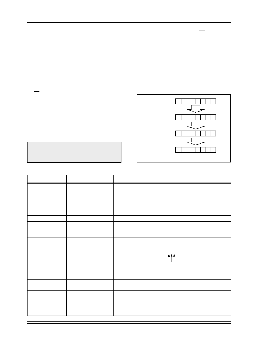
RX Status Instruction
The RX Status instruction (Figure 12-9) is used to
quickly determine which filter matched the message
and message type (standard, extended, remote). After
the command byte is sent, the controller will return
8 bits of data that contain the status data. If more clocks
are sent after the 8 bits are transmitted, the controller
will continue to output the same status bits as long as
the CS pin stays low and clocks are provided.
12.10 Bit Modify Instruction
The Bit Modify instruction provides a means for setting
or clearing individual bits in specific status and control
registers. This command is not available for all
registers. See Section 11.0 “Register Map” to
determine which registers allow the use of this
command.
The part is selected by lowering the CS pin and the Bit
Modify command byte is then sent to the MCP2515.
The command is followed by the address of the
register, the mask byte and finally the data byte.
The mask byte determines which bits in the register will
be allowed to change. A ‘1’ in the mask byte will allow
a bit in the register to change, while a ‘0’ will not.
The data byte determines what value the modified bits
in the register will be changed to. A ‘1’ in the data byte
will set the bit and a ‘0’ will clear the bit, provided that
the mask for that bit is set to a ‘1’ (see Figure 12-7).
FIGURE 12-1:
BIT MODIFY
TABLE 12-1:
SPI INSTRUCTION SET
Note:
Executing the Bit Modify command on
registers that are not bit-modifiable will
force the mask to FFh. This will allow byte-
writes to the registers, not bit modify.
Mask byte
Data byte
Previous
Register
Contents
Resulting
Register
Contents
00 1
1
11
00
XX 1
1
00
XX
01 0
1
10
00
01 1
1
00
Instruction Name
Instruction Format
Description
RESET
1100 0000
Resets internal registers to default state, set Configuration mode.
READ
0000 0011
Read data from register beginning at selected address.
Read RX Buffer
1001 0nm0
When reading a receive buffer, reduces the overhead of a normal
read command by placing the address pointer at one of four
locations, as indicated by ‘n,m’. Note: The associated RX flag bit
(CANINTF.RXnIF) will be cleared after bringing CS high.
WRITE
0000 0010
Write data to register beginning at selected address.
Load TX Buffer
0100 0abc
When loading a transmit buffer, reduces the overhead of a normal
Write command by placing the address pointer at one of six
locations as indicated by ‘a,b,c’.
RTS
(Message
Request-To-Send)
1000 0nnn
Instructs controller to begin message transmission sequence for
any of the transmit buffers.
Read Status
1010 0000
Quick polling command that reads several status bits for transmit
and receive functions.
RX Status
1011 0000
Quick polling command that indicates filter match and message
type (standard, extended and/or remote) of received message.
Bit Modify
0000 0101
Allows the user to set or clear individual bits in a particular
register. Note: Not all registers can be bit-modified with this
command. Executing this command on registers that are not bit-
modifiable will force the mask to FFh. See the register map in
Section 11.0 “Register Map” for a list of the registers that apply.
1000 0nnn
Request-to-send for TXBO
Request-to-send for TXB1
Request-to-send for TXB2
相关PDF资料 |
PDF描述 |
|---|---|
| V375A36E600B3 | CONVERTER MOD DC/DC 36V 600W |
| VE-JWH-IX-F1 | CONVERTER MOD DC/DC 52V 75W |
| PIC18F4610-I/ML | IC MCU FLASH 32KX16 44QFN |
| V375A36E600B2 | CONVERTER MOD DC/DC 36V 600W |
| VE-JWF-IX-F4 | CONVERTER MOD DC/DC 72V 75W |
相关代理商/技术参数 |
参数描述 |
|---|---|
| PIC18F2480-I/ML | 功能描述:8位微控制器 -MCU 16 KB 768 RAM 25 I/O RoHS:否 制造商:Silicon Labs 核心:8051 处理器系列:C8051F39x 数据总线宽度:8 bit 最大时钟频率:50 MHz 程序存储器大小:16 KB 数据 RAM 大小:1 KB 片上 ADC:Yes 工作电源电压:1.8 V to 3.6 V 工作温度范围:- 40 C to + 105 C 封装 / 箱体:QFN-20 安装风格:SMD/SMT |
| PIC18F2480-I/SO | 功能描述:8位微控制器 -MCU 16 KB 768 RAM 25 I/O RoHS:否 制造商:Silicon Labs 核心:8051 处理器系列:C8051F39x 数据总线宽度:8 bit 最大时钟频率:50 MHz 程序存储器大小:16 KB 数据 RAM 大小:1 KB 片上 ADC:Yes 工作电源电压:1.8 V to 3.6 V 工作温度范围:- 40 C to + 105 C 封装 / 箱体:QFN-20 安装风格:SMD/SMT |
| PIC18F2480-I/SP | 功能描述:8位微控制器 -MCU 16 KB 768 RAM 25 I/O RoHS:否 制造商:Silicon Labs 核心:8051 处理器系列:C8051F39x 数据总线宽度:8 bit 最大时钟频率:50 MHz 程序存储器大小:16 KB 数据 RAM 大小:1 KB 片上 ADC:Yes 工作电源电压:1.8 V to 3.6 V 工作温度范围:- 40 C to + 105 C 封装 / 箱体:QFN-20 安装风格:SMD/SMT |
| PIC18F2480T-I/ML | 功能描述:8位微控制器 -MCU 16 KB 768 RAM 25 I/O RoHS:否 制造商:Silicon Labs 核心:8051 处理器系列:C8051F39x 数据总线宽度:8 bit 最大时钟频率:50 MHz 程序存储器大小:16 KB 数据 RAM 大小:1 KB 片上 ADC:Yes 工作电源电压:1.8 V to 3.6 V 工作温度范围:- 40 C to + 105 C 封装 / 箱体:QFN-20 安装风格:SMD/SMT |
| PIC18F2480T-I/SO | 功能描述:8位微控制器 -MCU 16 KB 768 RAM 25 I/O RoHS:否 制造商:Silicon Labs 核心:8051 处理器系列:C8051F39x 数据总线宽度:8 bit 最大时钟频率:50 MHz 程序存储器大小:16 KB 数据 RAM 大小:1 KB 片上 ADC:Yes 工作电源电压:1.8 V to 3.6 V 工作温度范围:- 40 C to + 105 C 封装 / 箱体:QFN-20 安装风格:SMD/SMT |
发布紧急采购,3分钟左右您将得到回复。