- 您现在的位置:买卖IC网 > PDF目录11469 > PIC18F45J50T-I/ML (Microchip Technology)IC PIC MCU FLASH 32KB 44-QFN PDF资料下载
参数资料
| 型号: | PIC18F45J50T-I/ML |
| 厂商: | Microchip Technology |
| 文件页数: | 55/164页 |
| 文件大小: | 0K |
| 描述: | IC PIC MCU FLASH 32KB 44-QFN |
| 产品培训模块: | PIC18 J Series MCU Overview |
| 标准包装: | 1,600 |
| 系列: | PIC® XLP™ 18F |
| 核心处理器: | PIC |
| 芯体尺寸: | 8-位 |
| 速度: | 48MHz |
| 连通性: | I²C,SPI,UART/USART,USB |
| 外围设备: | 欠压检测/复位,DMA,POR,PWM,WDT |
| 输入/输出数: | 34 |
| 程序存储器容量: | 32KB(16K x 16) |
| 程序存储器类型: | 闪存 |
| RAM 容量: | 3.8K x 8 |
| 电压 - 电源 (Vcc/Vdd): | 2.15 V ~ 3.6 V |
| 数据转换器: | A/D 13x10b |
| 振荡器型: | 内部 |
| 工作温度: | -40°C ~ 85°C |
| 封装/外壳: | 44-VQFN 裸露焊盘 |
| 包装: | 带卷 (TR) |
第1页第2页第3页第4页第5页第6页第7页第8页第9页第10页第11页第12页第13页第14页第15页第16页第17页第18页第19页第20页第21页第22页第23页第24页第25页第26页第27页第28页第29页第30页第31页第32页第33页第34页第35页第36页第37页第38页第39页第40页第41页第42页第43页第44页第45页第46页第47页第48页第49页第50页第51页第52页第53页第54页当前第55页第56页第57页第58页第59页第60页第61页第62页第63页第64页第65页第66页第67页第68页第69页第70页第71页第72页第73页第74页第75页第76页第77页第78页第79页第80页第81页第82页第83页第84页第85页第86页第87页第88页第89页第90页第91页第92页第93页第94页第95页第96页第97页第98页第99页第100页第101页第102页第103页第104页第105页第106页第107页第108页第109页第110页第111页第112页第113页第114页第115页第116页第117页第118页第119页第120页第121页第122页第123页第124页第125页第126页第127页第128页第129页第130页第131页第132页第133页第134页第135页第136页第137页第138页第139页第140页第141页第142页第143页第144页第145页第146页第147页第148页第149页第150页第151页第152页第153页第154页第155页第156页第157页第158页第159页第160页第161页第162页第163页第164页
PIC18F46J50 FAMILY
DS39931D-page 148
2011 Microchip Technology Inc.
10.6
PORTE, TRISE and LATE
Registers
Depending on the particular PIC18F46J50 family
device selected, PORTE is implemented in two
different ways.
For 44-pin devices, PORTE is a 3-bit wide port. Three
pins (RE0/AN5/PMRD, RE1/AN6/PMWR and RE2/
AN7/PMCS) are individually configurable as inputs or
outputs. These pins have Schmitt Trigger input buffers.
When selected as analog inputs, these pins will read as
‘0’s.
The corresponding Data Direction register is TRISE.
Setting a TRISE bit (= 1) will make the corresponding
PORTE pin an input (i.e., put the corresponding output
driver in a High-Impedance mode). Clearing a TRISE
bit (= 0) will make the corresponding PORTE pin an
output (i.e., put the contents of the output latch on the
selected pin).
TRISE controls the direction of the RE pins, even when
they are being used as analog inputs. The user must
make sure to keep the pins configured as inputs when
using them as analog inputs.
The Data Latch register (LATE) is also memory
mapped. Read-modify-write operations on the LATE
register read and write the latched output value for
PORTE.
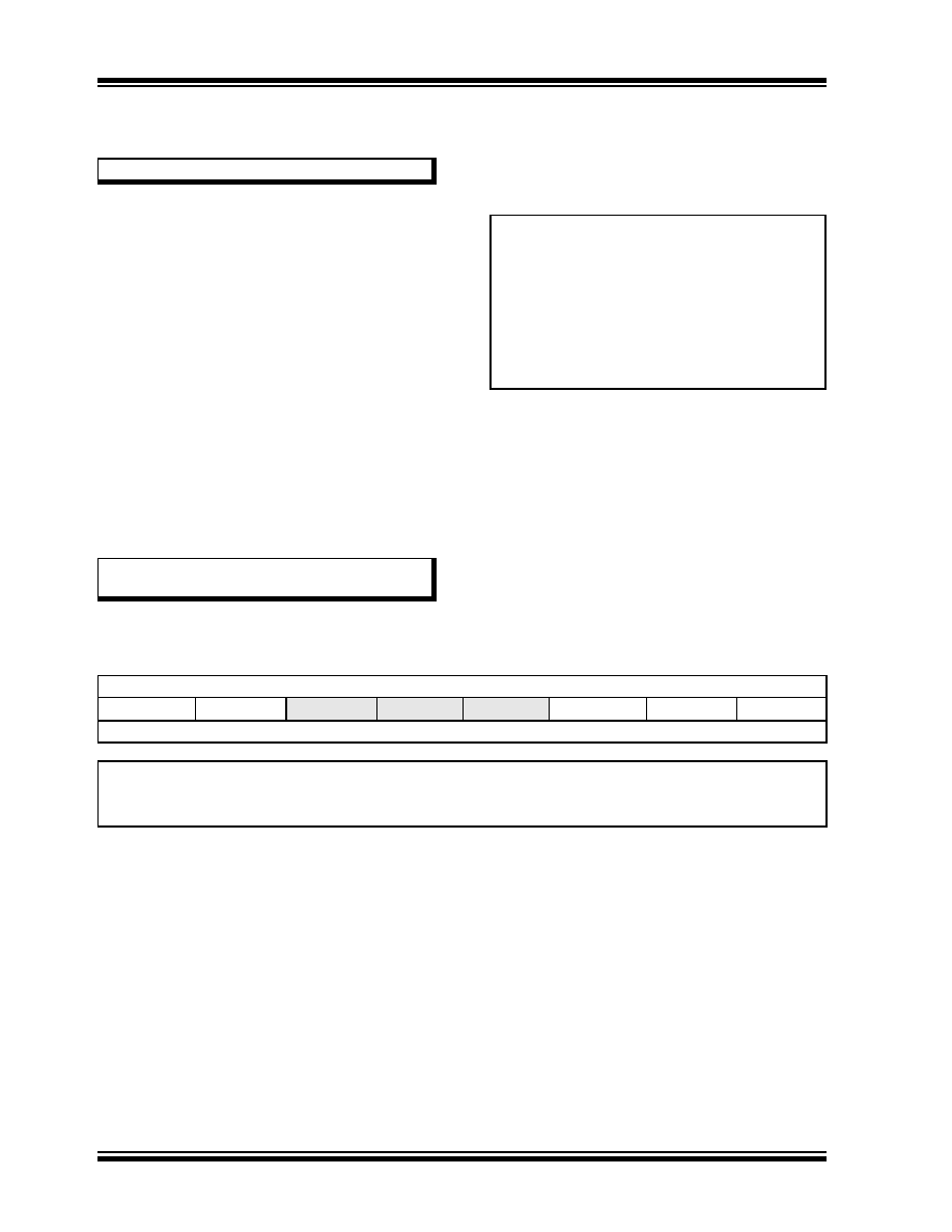
EXAMPLE 10-6:
INITIALIZING PORTE
Each of the PORTE pins has a weak internal pull-up. A
single control bit can turn on all the pull-ups. This is per-
formed by setting bit, REPU (PORTE<6>). The weak
pull-up is automatically turned off when the port pin is
configured as an output. The pull-ups are disabled on a
POR. The integrated weak pull-ups consist of a semi-
conductor structure similar to, but somewhat different,
from a discrete resistor. On an unloaded I/O pin, the
weak pull-ups are intended to provide logic high indica-
tion, but will not necessarily pull the pin all the way to
VDD levels.
Note that the pull-ups can be used for any set of
features, similar to the pull-ups found on PORTB
Note:
PORTE is available only on 44-pin devices.
Note:
On a POR, RE<2:0> are configured as
analog inputs.
CLRF
LATE
;Initialize LATE output
;latch values
MOVLB
0x0F
;ANCON registers not
;in access bank
BSF
ANCON0,PCFG5
;RE0/AN5 as digital
BSF
ANCON0,PCFG6
;RE1/AN6 as digital
MOVLW
0x03
;Example value used to
;initialize data direction
MOVWF
TRISE
;RE0, RE1 as inputs
;RE2 as output
REGISTER 10-5:
PORTE REGISTER
R/W-0
U-0
R/W-0
RDPU
REPU
—
RE2
RE1
RE0
bit 7
bit 0
Legend:
R = Readable bit
W = Writable bit
U = Unimplemented bit, read as ‘0’
-n = Value at POR
‘1’ = Bit is set
‘0’ = Bit is cleared
x = Bit is unknown
bit 7
RDPU:
PORTD Pull-up Enable bit
1
= PORTD pull-ups are enabled by individual TRIS values
0
= All PORTD pull-ups are disabled
bit 6
REPU:
PORTE Pull-up Enable bit
1
= PORTE pull-ups are enabled by individual TRIS values
0
= All PORTE pull-ups are disabled
bit 5-3
Unimplemented:
Read as ‘0’
bit 2-0
RE<2:0>:
PORTE Data Input bits
相关PDF资料 |
PDF描述 |
|---|---|
| PIC18LF45J50T-I/ML | IC PIC MCU FLASH 32KB 44-QFN |
| PIC24F32KA304T-I/PT | MCU 32KB FLASH 2KB RAM 44TQFP |
| PIC16LF1939-I/PT | IC MCU 8BIT FLASH 44TQFP |
| PIC24FV32KA304T-I/PT | MCU 32KB FLASH 2KB RAM 44TQFP |
| PIC18F45K80-E/ML | MCU PIC 32KB FLASH ECAN 44QFN |
相关代理商/技术参数 |
参数描述 |
|---|---|
| PIC18F45K20-E/ML | 功能描述:8位微控制器 -MCU 32KB Flash 1536B RAM 25 I/O 8B RoHS:否 制造商:Silicon Labs 核心:8051 处理器系列:C8051F39x 数据总线宽度:8 bit 最大时钟频率:50 MHz 程序存储器大小:16 KB 数据 RAM 大小:1 KB 片上 ADC:Yes 工作电源电压:1.8 V to 3.6 V 工作温度范围:- 40 C to + 105 C 封装 / 箱体:QFN-20 安装风格:SMD/SMT |
| PIC18F45K20-E/MV | 功能描述:8位微控制器 -MCU 32KB FL 1536b RAM 8b Familynanowatt XLP RoHS:否 制造商:Silicon Labs 核心:8051 处理器系列:C8051F39x 数据总线宽度:8 bit 最大时钟频率:50 MHz 程序存储器大小:16 KB 数据 RAM 大小:1 KB 片上 ADC:Yes 工作电源电压:1.8 V to 3.6 V 工作温度范围:- 40 C to + 105 C 封装 / 箱体:QFN-20 安装风格:SMD/SMT |
| PIC18F45K20-E/P | 功能描述:8位微控制器 -MCU 32KB Flash 1536B RAM 25 I/O 8B RoHS:否 制造商:Silicon Labs 核心:8051 处理器系列:C8051F39x 数据总线宽度:8 bit 最大时钟频率:50 MHz 程序存储器大小:16 KB 数据 RAM 大小:1 KB 片上 ADC:Yes 工作电源电压:1.8 V to 3.6 V 工作温度范围:- 40 C to + 105 C 封装 / 箱体:QFN-20 安装风格:SMD/SMT |
| PIC18F45K20-E/PT | 功能描述:8位微控制器 -MCU 32KB Flash 1536B RAM 25 I/O 8B RoHS:否 制造商:Silicon Labs 核心:8051 处理器系列:C8051F39x 数据总线宽度:8 bit 最大时钟频率:50 MHz 程序存储器大小:16 KB 数据 RAM 大小:1 KB 片上 ADC:Yes 工作电源电压:1.8 V to 3.6 V 工作温度范围:- 40 C to + 105 C 封装 / 箱体:QFN-20 安装风格:SMD/SMT |
| PIC18F45K20-I/ML | 功能描述:8位微控制器 -MCU 32KB Flash 1536B RAM 25 I/O 8B RoHS:否 制造商:Silicon Labs 核心:8051 处理器系列:C8051F39x 数据总线宽度:8 bit 最大时钟频率:50 MHz 程序存储器大小:16 KB 数据 RAM 大小:1 KB 片上 ADC:Yes 工作电源电压:1.8 V to 3.6 V 工作温度范围:- 40 C to + 105 C 封装 / 箱体:QFN-20 安装风格:SMD/SMT |
发布紧急采购,3分钟左右您将得到回复。