- 您现在的位置:买卖IC网 > PDF目录11469 > PIC18F45J50T-I/ML (Microchip Technology)IC PIC MCU FLASH 32KB 44-QFN PDF资料下载
参数资料
| 型号: | PIC18F45J50T-I/ML |
| 厂商: | Microchip Technology |
| 文件页数: | 7/164页 |
| 文件大小: | 0K |
| 描述: | IC PIC MCU FLASH 32KB 44-QFN |
| 产品培训模块: | PIC18 J Series MCU Overview |
| 标准包装: | 1,600 |
| 系列: | PIC® XLP™ 18F |
| 核心处理器: | PIC |
| 芯体尺寸: | 8-位 |
| 速度: | 48MHz |
| 连通性: | I²C,SPI,UART/USART,USB |
| 外围设备: | 欠压检测/复位,DMA,POR,PWM,WDT |
| 输入/输出数: | 34 |
| 程序存储器容量: | 32KB(16K x 16) |
| 程序存储器类型: | 闪存 |
| RAM 容量: | 3.8K x 8 |
| 电压 - 电源 (Vcc/Vdd): | 2.15 V ~ 3.6 V |
| 数据转换器: | A/D 13x10b |
| 振荡器型: | 内部 |
| 工作温度: | -40°C ~ 85°C |
| 封装/外壳: | 44-VQFN 裸露焊盘 |
| 包装: | 带卷 (TR) |
第1页第2页第3页第4页第5页第6页当前第7页第8页第9页第10页第11页第12页第13页第14页第15页第16页第17页第18页第19页第20页第21页第22页第23页第24页第25页第26页第27页第28页第29页第30页第31页第32页第33页第34页第35页第36页第37页第38页第39页第40页第41页第42页第43页第44页第45页第46页第47页第48页第49页第50页第51页第52页第53页第54页第55页第56页第57页第58页第59页第60页第61页第62页第63页第64页第65页第66页第67页第68页第69页第70页第71页第72页第73页第74页第75页第76页第77页第78页第79页第80页第81页第82页第83页第84页第85页第86页第87页第88页第89页第90页第91页第92页第93页第94页第95页第96页第97页第98页第99页第100页第101页第102页第103页第104页第105页第106页第107页第108页第109页第110页第111页第112页第113页第114页第115页第116页第117页第118页第119页第120页第121页第122页第123页第124页第125页第126页第127页第128页第129页第130页第131页第132页第133页第134页第135页第136页第137页第138页第139页第140页第141页第142页第143页第144页第145页第146页第147页第148页第149页第150页第151页第152页第153页第154页第155页第156页第157页第158页第159页第160页第161页第162页第163页第164页
PIC18F46J50 FAMILY
DS39931D-page 104
2011 Microchip Technology Inc.
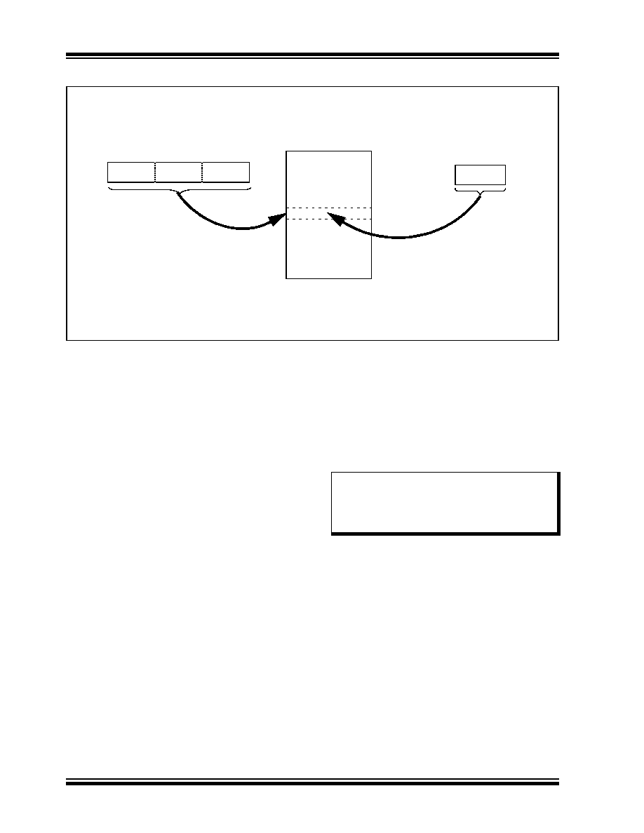
FIGURE 7-2:
TABLE WRITE OPERATION
7.2
Control Registers
Several control registers are used in conjunction with
the TBLRD and TBLWT instructions. Those are:
EECON1 register
EECON2 register
TABLAT register
TBLPTR registers
7.2.1
EECON1 AND EECON2 REGISTERS
The EECON1 register (Register 7-1) is the control
register for memory accesses. The EECON2 register is
not a physical register; it is used exclusively in the
memory write and erase sequences. Reading
EECON2 will read all ‘0’s.
The WPROG bit, when set, will allow programming
two bytes per word on the execution of the WR
command. If this bit is cleared, the WR command will
result in programming on a block of 64 bytes.
The FREE bit, when set, will allow a program memory
erase operation. When FREE is set, the erase
operation is initiated on the next WR command. When
FREE is clear, only writes are enabled.
The WREN bit, when set, will allow a write operation.
On power-up, the WREN bit is clear. The WRERR bit is
set in hardware when the WR bit is set and cleared
when the internal programming timer expires and the
write operation is complete.
The WR control bit initiates write operations. The bit
cannot be cleared, only set, in software. It is cleared in
hardware at the completion of the write operation.
Table Pointer(1)
Table Latch (8-bit)
TBLPTRH
TBLPTRL
TABLAT
Program Memory
(TBLPTR)
TBLPTRU
Instruction: TBLWT*
Note
1:
The Table Pointer actually points to one of 64 holding registers, the address of which is determined by
TBLPTRL<5:0>. The process for physically writing data to the program memory array is discussed in
.
Holding Registers
Program Memory
Note:
During normal operation, the WRERR is
read as ‘1’. This can indicate that a write
operation was prematurely terminated by
a Reset, or a write operation was
attempted improperly.
相关PDF资料 |
PDF描述 |
|---|---|
| PIC18LF45J50T-I/ML | IC PIC MCU FLASH 32KB 44-QFN |
| PIC24F32KA304T-I/PT | MCU 32KB FLASH 2KB RAM 44TQFP |
| PIC16LF1939-I/PT | IC MCU 8BIT FLASH 44TQFP |
| PIC24FV32KA304T-I/PT | MCU 32KB FLASH 2KB RAM 44TQFP |
| PIC18F45K80-E/ML | MCU PIC 32KB FLASH ECAN 44QFN |
相关代理商/技术参数 |
参数描述 |
|---|---|
| PIC18F45K20-E/ML | 功能描述:8位微控制器 -MCU 32KB Flash 1536B RAM 25 I/O 8B RoHS:否 制造商:Silicon Labs 核心:8051 处理器系列:C8051F39x 数据总线宽度:8 bit 最大时钟频率:50 MHz 程序存储器大小:16 KB 数据 RAM 大小:1 KB 片上 ADC:Yes 工作电源电压:1.8 V to 3.6 V 工作温度范围:- 40 C to + 105 C 封装 / 箱体:QFN-20 安装风格:SMD/SMT |
| PIC18F45K20-E/MV | 功能描述:8位微控制器 -MCU 32KB FL 1536b RAM 8b Familynanowatt XLP RoHS:否 制造商:Silicon Labs 核心:8051 处理器系列:C8051F39x 数据总线宽度:8 bit 最大时钟频率:50 MHz 程序存储器大小:16 KB 数据 RAM 大小:1 KB 片上 ADC:Yes 工作电源电压:1.8 V to 3.6 V 工作温度范围:- 40 C to + 105 C 封装 / 箱体:QFN-20 安装风格:SMD/SMT |
| PIC18F45K20-E/P | 功能描述:8位微控制器 -MCU 32KB Flash 1536B RAM 25 I/O 8B RoHS:否 制造商:Silicon Labs 核心:8051 处理器系列:C8051F39x 数据总线宽度:8 bit 最大时钟频率:50 MHz 程序存储器大小:16 KB 数据 RAM 大小:1 KB 片上 ADC:Yes 工作电源电压:1.8 V to 3.6 V 工作温度范围:- 40 C to + 105 C 封装 / 箱体:QFN-20 安装风格:SMD/SMT |
| PIC18F45K20-E/PT | 功能描述:8位微控制器 -MCU 32KB Flash 1536B RAM 25 I/O 8B RoHS:否 制造商:Silicon Labs 核心:8051 处理器系列:C8051F39x 数据总线宽度:8 bit 最大时钟频率:50 MHz 程序存储器大小:16 KB 数据 RAM 大小:1 KB 片上 ADC:Yes 工作电源电压:1.8 V to 3.6 V 工作温度范围:- 40 C to + 105 C 封装 / 箱体:QFN-20 安装风格:SMD/SMT |
| PIC18F45K20-I/ML | 功能描述:8位微控制器 -MCU 32KB Flash 1536B RAM 25 I/O 8B RoHS:否 制造商:Silicon Labs 核心:8051 处理器系列:C8051F39x 数据总线宽度:8 bit 最大时钟频率:50 MHz 程序存储器大小:16 KB 数据 RAM 大小:1 KB 片上 ADC:Yes 工作电源电压:1.8 V to 3.6 V 工作温度范围:- 40 C to + 105 C 封装 / 箱体:QFN-20 安装风格:SMD/SMT |
发布紧急采购,3分钟左右您将得到回复。