- 您现在的位置:买卖IC网 > PDF目录3868 > PIC18F66J16-I/PT (Microchip Technology)IC PIC MCU FLASH 48KX16 64TQFP PDF资料下载
参数资料
| 型号: | PIC18F66J16-I/PT |
| 厂商: | Microchip Technology |
| 文件页数: | 46/107页 |
| 文件大小: | 0K |
| 描述: | IC PIC MCU FLASH 48KX16 64TQFP |
| 产品培训模块: | Asynchronous Stimulus PIC18 J Series MCU Overview 8-bit PIC® Microcontroller Portfolio |
| 标准包装: | 160 |
| 系列: | PIC® 18F |
| 核心处理器: | PIC |
| 芯体尺寸: | 8-位 |
| 速度: | 48MHz |
| 连通性: | I²C,SPI,UART/USART |
| 外围设备: | 欠压检测/复位,LVD,POR,PWM,WDT |
| 输入/输出数: | 52 |
| 程序存储器容量: | 96KB(48K x 16) |
| 程序存储器类型: | 闪存 |
| RAM 容量: | 3930 x 8 |
| 电压 - 电源 (Vcc/Vdd): | 2 V ~ 3.6 V |
| 数据转换器: | A/D 11x10b |
| 振荡器型: | 内部 |
| 工作温度: | -40°C ~ 85°C |
| 封装/外壳: | 64-TQFP |
| 包装: | 托盘 |
| 产品目录页面: | 644 (CN2011-ZH PDF) |
| 配用: | AC162091-ND - HEADER MPLAB ICD2 18F87J11 64/80 MA180020-ND - MODULE PLUG-IN HPC EXPL 18F87J11 AC164327-ND - MODULE SKT FOR 64TQFP |
第1页第2页第3页第4页第5页第6页第7页第8页第9页第10页第11页第12页第13页第14页第15页第16页第17页第18页第19页第20页第21页第22页第23页第24页第25页第26页第27页第28页第29页第30页第31页第32页第33页第34页第35页第36页第37页第38页第39页第40页第41页第42页第43页第44页第45页当前第46页第47页第48页第49页第50页第51页第52页第53页第54页第55页第56页第57页第58页第59页第60页第61页第62页第63页第64页第65页第66页第67页第68页第69页第70页第71页第72页第73页第74页第75页第76页第77页第78页第79页第80页第81页第82页第83页第84页第85页第86页第87页第88页第89页第90页第91页第92页第93页第94页第95页第96页第97页第98页第99页第100页第101页第102页第103页第104页第105页第106页第107页
2007-2012 Microchip Technology Inc.
DS39778E-page 43
PIC18F87J11 FAMILY
3.5
Internal Oscillator Block
The PIC18F87J11 family of devices includes an
internal oscillator block which generates two different
clock signals; either can be used as the microcon-
troller’s clock source. This may eliminate the need for
an external oscillator circuit on the OSC1 and/or OSC2
pins.
The main output is the Fast RC oscillator, or INTOSC,
an 8 MHz clock source which can be used to directly
drive the device clock. It also drives a postscaler, which
can provide a range of clock frequencies from 31 kHz
to 4 MHz. INTOSC is enabled when a clock frequency
from 125 kHz to 8 MHz is selected. The INTOSC out-
put can also be enabled when 31 kHz is selected,
depending on the INTSRC bit (OSCTUNE<7>).
The other clock source is the internal RC oscillator
(INTRC), which provides a nominal 31 kHz output.
INTRC is enabled if it is selected as the device clock
source; it is also enabled automatically when any of the
following are enabled:
Power-up Timer
Fail-Safe Clock Monitor
Watchdog Timer
Two-Speed Start-up
These features are discussed in greater detail in
The clock source frequency (INTOSC direct, INTOSC
with postscaler or INTRC direct) is selected by config-
uring the IRCFx bits of the OSCCON register. The
default frequency on device Resets is 4 MHz.
3.5.1
INTIO MODES
Using the internal oscillator as the clock source elimi-
nates the need for up to two external oscillator pins,
which can then be used for digital I/O. Two distinct
oscillator configurations, which are determined by the
FOSCx Configuration bits, are available:
In INTIO1 mode, the OSC2 pin outputs FOSC/4,
while OSC1 functions as RA7 (see Figure 3-6) for
digital input and output.
In INTIO2 mode, OSC1 functions as RA7 and
OSC2 functions as RA6 (see Figure 3-7), both for
digital input and output.
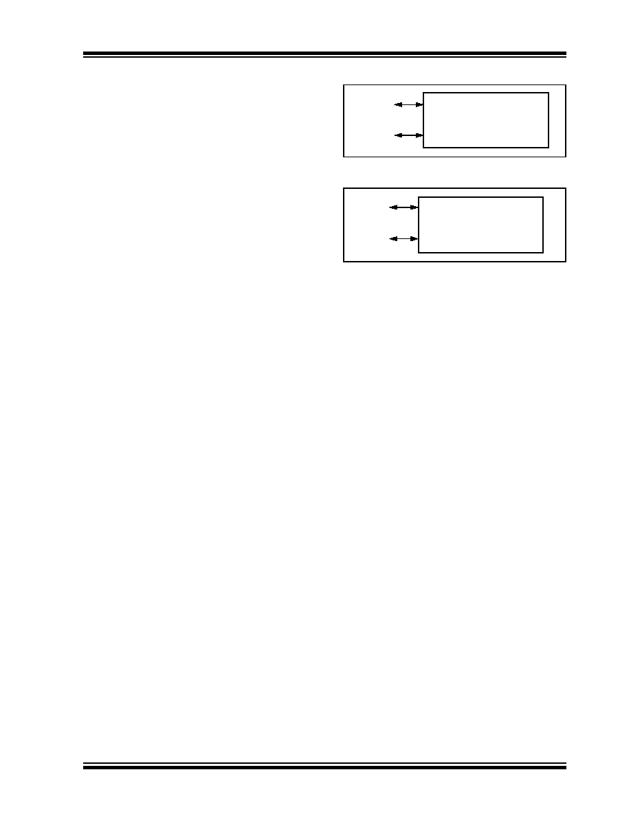
FIGURE 3-6:
INTIO1 OSCILLATOR MODE
FIGURE 3-7:
INTIO2 OSCILLATOR MODE
3.5.2
INTPLL MODES
The 4x Phase Locked Loop (PLL) can be used with the
internal oscillator block to produce faster device clock
speeds than are normally possible with the internal
oscillator sources. When enabled, the PLL produces a
clock speed of 16 MHz or 32 MHz.
PLL operation is controlled through software. The con-
trol bit, PLLEN (OSCTUNE<6>), is used to enable or
disable its operation. The PLL is available only to
INTOSC when the device is configured to use one of
the INTPLL modes as the primary clock source
(FOSC<2:0> = 011 or 010). Additionally, the PLL will
only function when the selected output frequency is
either 4 MHz or 8 MHz (OSCCON<6:4> = 111 or 110).
Like the INTIO modes, there are two distinct INTPLL
modes available:
In INTPLL1 mode, the OSC2 pin outputs FOSC/4,
while OSC1 functions as RA7 for digital input and
output. Externally, this is identical in appearance
to INTIO1 (Figure 3-6).
In INTPLL2 mode, OSC1 functions as RA7 and
OSC2 functions as RA6, both for digital input and
output. Externally, this is identical to INTIO2
PIC18F87J11
OSC2
FOSC/4
I/O (OSC1)
RA7
PIC18F87J11
I/O (OSC2)
RA6
I/O (OSC1)
RA7
相关PDF资料 |
PDF描述 |
|---|---|
| PIC18LF24J50-I/SS | IC PIC MCU FLASH 16K 2V 28-SSOP |
| PIC18F24J50-I/SS | IC PIC MCU FLASH 16K 2V 28-SSOP |
| PIC24FV16KA301-I/SS | MCU 16KB FLASH 2KB RAM 20-SSOP |
| PIC24FJ32GA002-I/ML | IC PIC MCU FLASH 32KB 28QFN |
| PIC24FJ16MC102-I/SP | IC MCU 16BIT 16KB FLASH 28SPDIP |
相关代理商/技术参数 |
参数描述 |
|---|---|
| PIC18F66J16T-I/PT | 功能描述:8位微控制器 -MCU 96KB Flash 3936 bytesRAM 51I/O RoHS:否 制造商:Silicon Labs 核心:8051 处理器系列:C8051F39x 数据总线宽度:8 bit 最大时钟频率:50 MHz 程序存储器大小:16 KB 数据 RAM 大小:1 KB 片上 ADC:Yes 工作电源电压:1.8 V to 3.6 V 工作温度范围:- 40 C to + 105 C 封装 / 箱体:QFN-20 安装风格:SMD/SMT |
| PIC18F66J50-I/PT | 功能描述:8位微控制器 -MCU 64KB FLSH 3936Bs RAM USB 2.0 nanoWatt RoHS:否 制造商:Silicon Labs 核心:8051 处理器系列:C8051F39x 数据总线宽度:8 bit 最大时钟频率:50 MHz 程序存储器大小:16 KB 数据 RAM 大小:1 KB 片上 ADC:Yes 工作电源电压:1.8 V to 3.6 V 工作温度范围:- 40 C to + 105 C 封装 / 箱体:QFN-20 安装风格:SMD/SMT |
| PIC18F66J50T-I/PT | 功能描述:8位微控制器 -MCU 64KB FLSH 3936Bs RAM USB 2.0 nanoWatt RoHS:否 制造商:Silicon Labs 核心:8051 处理器系列:C8051F39x 数据总线宽度:8 bit 最大时钟频率:50 MHz 程序存储器大小:16 KB 数据 RAM 大小:1 KB 片上 ADC:Yes 工作电源电压:1.8 V to 3.6 V 工作温度范围:- 40 C to + 105 C 封装 / 箱体:QFN-20 安装风格:SMD/SMT |
| PIC18F66J55-I/PT | 功能描述:8位微控制器 -MCU 96KB FLSH 3936Bs RAM USB 2.0 nanoWatt RoHS:否 制造商:Silicon Labs 核心:8051 处理器系列:C8051F39x 数据总线宽度:8 bit 最大时钟频率:50 MHz 程序存储器大小:16 KB 数据 RAM 大小:1 KB 片上 ADC:Yes 工作电源电压:1.8 V to 3.6 V 工作温度范围:- 40 C to + 105 C 封装 / 箱体:QFN-20 安装风格:SMD/SMT |
| PIC18F66J55T-I/PT | 功能描述:8位微控制器 -MCU 96KB FLSH 3936Bs RAM USB 2.0 nanoWatt RoHS:否 制造商:Silicon Labs 核心:8051 处理器系列:C8051F39x 数据总线宽度:8 bit 最大时钟频率:50 MHz 程序存储器大小:16 KB 数据 RAM 大小:1 KB 片上 ADC:Yes 工作电源电压:1.8 V to 3.6 V 工作温度范围:- 40 C to + 105 C 封装 / 箱体:QFN-20 安装风格:SMD/SMT |
发布紧急采购,3分钟左右您将得到回复。