- 您现在的位置:买卖IC网 > PDF目录3868 > PIC18F66J16-I/PT (Microchip Technology)IC PIC MCU FLASH 48KX16 64TQFP PDF资料下载
参数资料
| 型号: | PIC18F66J16-I/PT |
| 厂商: | Microchip Technology |
| 文件页数: | 77/107页 |
| 文件大小: | 0K |
| 描述: | IC PIC MCU FLASH 48KX16 64TQFP |
| 产品培训模块: | Asynchronous Stimulus PIC18 J Series MCU Overview 8-bit PIC® Microcontroller Portfolio |
| 标准包装: | 160 |
| 系列: | PIC® 18F |
| 核心处理器: | PIC |
| 芯体尺寸: | 8-位 |
| 速度: | 48MHz |
| 连通性: | I²C,SPI,UART/USART |
| 外围设备: | 欠压检测/复位,LVD,POR,PWM,WDT |
| 输入/输出数: | 52 |
| 程序存储器容量: | 96KB(48K x 16) |
| 程序存储器类型: | 闪存 |
| RAM 容量: | 3930 x 8 |
| 电压 - 电源 (Vcc/Vdd): | 2 V ~ 3.6 V |
| 数据转换器: | A/D 11x10b |
| 振荡器型: | 内部 |
| 工作温度: | -40°C ~ 85°C |
| 封装/外壳: | 64-TQFP |
| 包装: | 托盘 |
| 产品目录页面: | 644 (CN2011-ZH PDF) |
| 配用: | AC162091-ND - HEADER MPLAB ICD2 18F87J11 64/80 MA180020-ND - MODULE PLUG-IN HPC EXPL 18F87J11 AC164327-ND - MODULE SKT FOR 64TQFP |
第1页第2页第3页第4页第5页第6页第7页第8页第9页第10页第11页第12页第13页第14页第15页第16页第17页第18页第19页第20页第21页第22页第23页第24页第25页第26页第27页第28页第29页第30页第31页第32页第33页第34页第35页第36页第37页第38页第39页第40页第41页第42页第43页第44页第45页第46页第47页第48页第49页第50页第51页第52页第53页第54页第55页第56页第57页第58页第59页第60页第61页第62页第63页第64页第65页第66页第67页第68页第69页第70页第71页第72页第73页第74页第75页第76页当前第77页第78页第79页第80页第81页第82页第83页第84页第85页第86页第87页第88页第89页第90页第91页第92页第93页第94页第95页第96页第97页第98页第99页第100页第101页第102页第103页第104页第105页第106页第107页
2007-2012 Microchip Technology Inc.
DS39778E-page 71
PIC18F87J11 FAMILY
6.1.5
PROGRAM COUNTER
The Program Counter (PC) specifies the address of the
instruction to fetch for execution. The PC is 21 bits wide
and is contained in three separate 8-bit registers. The
low byte, known as the PCL register, is both readable
and writable. The high byte, or PCH register, contains
the PC<15:8> bits; it is not directly readable or writable.
Updates to the PCH register are performed through the
PCLATH register. The upper byte is called PCU. This
register contains the PC<20:16> bits; it is also not
directly readable or writable. Updates to the PCU
register are performed through the PCLATU register.
The contents of PCLATH and PCLATU are transferred
to the Program Counter by any operation that writes
PCL. Similarly, the upper two bytes of the Program
Counter are transferred to PCLATH and PCLATU by an
operation that reads PCL. This is useful for computed
offsets to the PC (see Section 6.1.8.1 “Computed
The PC addresses bytes in the program memory. To
prevent the PC from becoming misaligned with word
instructions, the Least Significant bit of PCL is fixed to
a value of ‘0’. The PC increments by 2 to address
sequential instructions in the program memory.
The CALL, RCALL, GOTO and program branch
instructions write to the Program Counter directly. For
these instructions, the contents of PCLATH and
PCLATU are not transferred to the Program Counter.
6.1.6
RETURN ADDRESS STACK
The return address stack allows any combination of up
to 31 program calls and interrupts to occur. The PC is
pushed onto the stack when a CALL or RCALL instruc-
tion is executed, or an interrupt is Acknowledged. The
PC value is pulled off the stack on a RETURN, RETLW
or a RETFIE instruction (and on ADDULNK and
SUBULNK
instructions if the extended instruction set is
enabled). PCLATU and PCLATH are not affected by
any of the RETURN or CALL instructions.
The stack operates as a 31-word by 21-bit RAM and a
5-bit Stack Pointer, STKPTR. The stack space is not
part of either program or data space. The Stack Pointer
is readable and writable and the address on the top of
the stack is readable and writable through the
Top-of-Stack Special Function Registers. Data can also
be pushed to, or popped from, the stack using these
registers.
A CALL type instruction causes a push onto the stack.
The Stack Pointer is first incremented and the location
pointed to by the Stack Pointer is written with the
contents of the PC (already pointing to the instruction
following the CALL). A RETURN type instruction causes
a pop from the stack. The contents of the location
pointed to by the STKPTR are transferred to the PC
and then the Stack Pointer is decremented.
The Stack Pointer is initialized to ‘00000’ after all
Resets. There is no RAM associated with the location
corresponding to a Stack Pointer value of ‘00000’; this
is only a Reset value. Status bits indicate if the stack is
full, has overflowed or has underflowed.
6.1.6.1
Top-of-Stack (TOS) Access
Only the top of the return address stack is readable and
writable. A set of three registers, TOSU:TOSH:TOSL,
hold the contents of the stack location pointed to by the
STKPTR register (Figure 6-4). This allows users to
implement a software stack if necessary. After a CALL,
RCALL
or interrupt (and ADDULNK and SUBULNK
instructions if the extended instruction set is enabled),
the software can read the pushed value by reading the
TOSU:TOSH:TOSL registers. These values can be
placed on a user-defined software stack. At return
time, the software can return these values to
TOSU:TOSH:TOSL and do a return.
The user must disable the Global Interrupt Enable bits
while accessing the stack to prevent inadvertent stack
corruption.
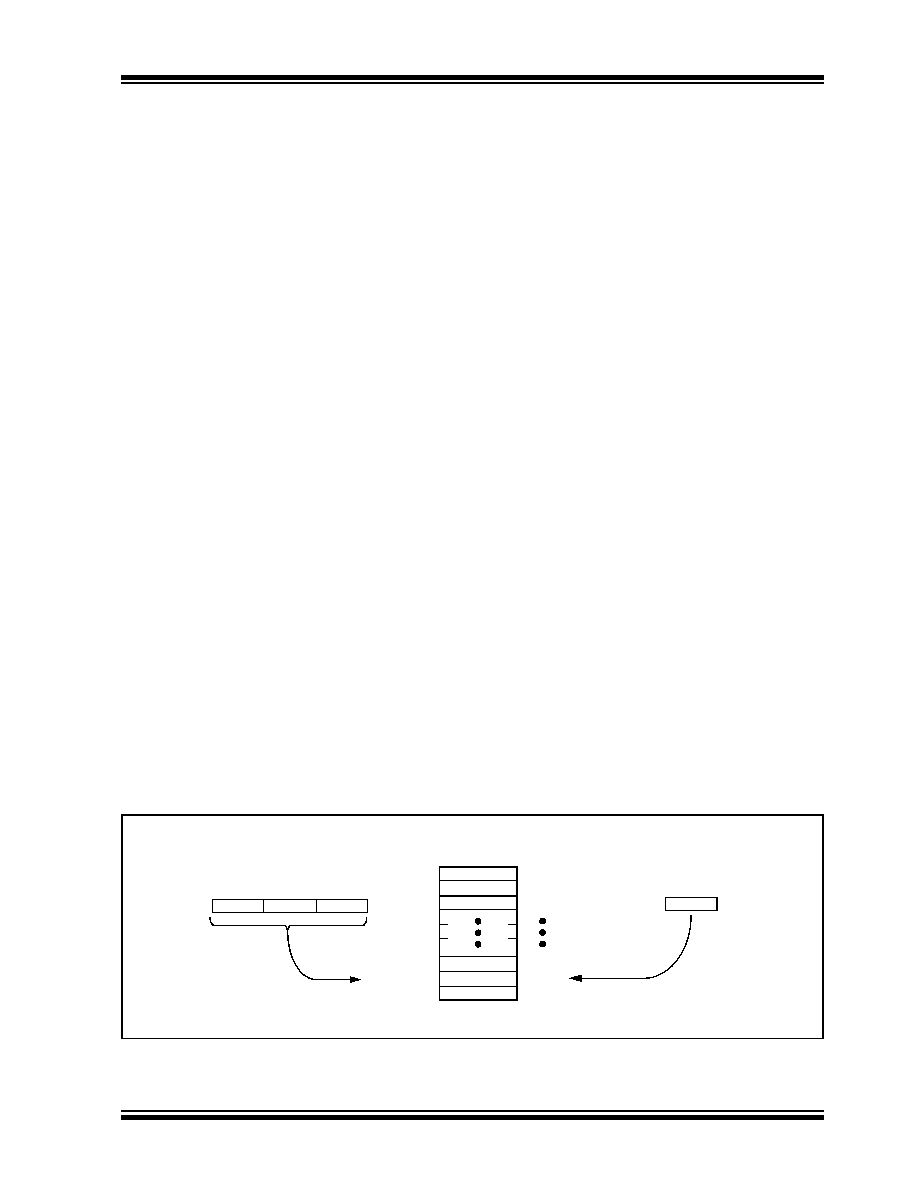
FIGURE 6-4:
RETURN ADDRESS STACK AND ASSOCIATED REGISTERS
00011
001A34h
11111
11110
11101
00010
00001
00000
00010
Return Address Stack <20:0>
Top-of-Stack
000D58h
TOSL
TOSH
TOSU
34h
1Ah
00h
STKPTR<4:0>
Top-of-Stack Registers
Stack Pointer
相关PDF资料 |
PDF描述 |
|---|---|
| PIC18LF24J50-I/SS | IC PIC MCU FLASH 16K 2V 28-SSOP |
| PIC18F24J50-I/SS | IC PIC MCU FLASH 16K 2V 28-SSOP |
| PIC24FV16KA301-I/SS | MCU 16KB FLASH 2KB RAM 20-SSOP |
| PIC24FJ32GA002-I/ML | IC PIC MCU FLASH 32KB 28QFN |
| PIC24FJ16MC102-I/SP | IC MCU 16BIT 16KB FLASH 28SPDIP |
相关代理商/技术参数 |
参数描述 |
|---|---|
| PIC18F66J16T-I/PT | 功能描述:8位微控制器 -MCU 96KB Flash 3936 bytesRAM 51I/O RoHS:否 制造商:Silicon Labs 核心:8051 处理器系列:C8051F39x 数据总线宽度:8 bit 最大时钟频率:50 MHz 程序存储器大小:16 KB 数据 RAM 大小:1 KB 片上 ADC:Yes 工作电源电压:1.8 V to 3.6 V 工作温度范围:- 40 C to + 105 C 封装 / 箱体:QFN-20 安装风格:SMD/SMT |
| PIC18F66J50-I/PT | 功能描述:8位微控制器 -MCU 64KB FLSH 3936Bs RAM USB 2.0 nanoWatt RoHS:否 制造商:Silicon Labs 核心:8051 处理器系列:C8051F39x 数据总线宽度:8 bit 最大时钟频率:50 MHz 程序存储器大小:16 KB 数据 RAM 大小:1 KB 片上 ADC:Yes 工作电源电压:1.8 V to 3.6 V 工作温度范围:- 40 C to + 105 C 封装 / 箱体:QFN-20 安装风格:SMD/SMT |
| PIC18F66J50T-I/PT | 功能描述:8位微控制器 -MCU 64KB FLSH 3936Bs RAM USB 2.0 nanoWatt RoHS:否 制造商:Silicon Labs 核心:8051 处理器系列:C8051F39x 数据总线宽度:8 bit 最大时钟频率:50 MHz 程序存储器大小:16 KB 数据 RAM 大小:1 KB 片上 ADC:Yes 工作电源电压:1.8 V to 3.6 V 工作温度范围:- 40 C to + 105 C 封装 / 箱体:QFN-20 安装风格:SMD/SMT |
| PIC18F66J55-I/PT | 功能描述:8位微控制器 -MCU 96KB FLSH 3936Bs RAM USB 2.0 nanoWatt RoHS:否 制造商:Silicon Labs 核心:8051 处理器系列:C8051F39x 数据总线宽度:8 bit 最大时钟频率:50 MHz 程序存储器大小:16 KB 数据 RAM 大小:1 KB 片上 ADC:Yes 工作电源电压:1.8 V to 3.6 V 工作温度范围:- 40 C to + 105 C 封装 / 箱体:QFN-20 安装风格:SMD/SMT |
| PIC18F66J55T-I/PT | 功能描述:8位微控制器 -MCU 96KB FLSH 3936Bs RAM USB 2.0 nanoWatt RoHS:否 制造商:Silicon Labs 核心:8051 处理器系列:C8051F39x 数据总线宽度:8 bit 最大时钟频率:50 MHz 程序存储器大小:16 KB 数据 RAM 大小:1 KB 片上 ADC:Yes 工作电源电压:1.8 V to 3.6 V 工作温度范围:- 40 C to + 105 C 封装 / 箱体:QFN-20 安装风格:SMD/SMT |
发布紧急采购,3分钟左右您将得到回复。