- 您现在的位置:买卖IC网 > PDF目录3892 > PIC18LC858-I/PT (Microchip Technology)IC MCU OTP 16KX16 CAN 80TQFP PDF资料下载
参数资料
| 型号: | PIC18LC858-I/PT |
| 厂商: | Microchip Technology |
| 文件页数: | 54/246页 |
| 文件大小: | 0K |
| 描述: | IC MCU OTP 16KX16 CAN 80TQFP |
| 标准包装: | 119 |
| 系列: | PIC® 18C |
| 核心处理器: | PIC |
| 芯体尺寸: | 8-位 |
| 速度: | 40MHz |
| 连通性: | CAN,I²C,SPI,UART/USART |
| 外围设备: | 欠压检测/复位,LVD,POR,PWM,WDT |
| 输入/输出数: | 68 |
| 程序存储器容量: | 32KB(16K x 16) |
| 程序存储器类型: | OTP |
| RAM 容量: | 1.5K x 8 |
| 电压 - 电源 (Vcc/Vdd): | 2.5 V ~ 5.5 V |
| 数据转换器: | A/D 16x10b |
| 振荡器型: | 外部 |
| 工作温度: | -40°C ~ 85°C |
| 封装/外壳: | 80-TQFP |
| 包装: | 托盘 |
| 其它名称: | PIC18LC858I/PT |
第1页第2页第3页第4页第5页第6页第7页第8页第9页第10页第11页第12页第13页第14页第15页第16页第17页第18页第19页第20页第21页第22页第23页第24页第25页第26页第27页第28页第29页第30页第31页第32页第33页第34页第35页第36页第37页第38页第39页第40页第41页第42页第43页第44页第45页第46页第47页第48页第49页第50页第51页第52页第53页当前第54页第55页第56页第57页第58页第59页第60页第61页第62页第63页第64页第65页第66页第67页第68页第69页第70页第71页第72页第73页第74页第75页第76页第77页第78页第79页第80页第81页第82页第83页第84页第85页第86页第87页第88页第89页第90页第91页第92页第93页第94页第95页第96页第97页第98页第99页第100页第101页第102页第103页第104页第105页第106页第107页第108页第109页第110页第111页第112页第113页第114页第115页第116页第117页第118页第119页第120页第121页第122页第123页第124页第125页第126页第127页第128页第129页第130页第131页第132页第133页第134页第135页第136页第137页第138页第139页第140页第141页第142页第143页第144页第145页第146页第147页第148页第149页第150页第151页第152页第153页第154页第155页第156页第157页第158页第159页第160页第161页第162页第163页第164页第165页第166页第167页第168页第169页第170页第171页第172页第173页第174页第175页第176页第177页第178页第179页第180页第181页第182页第183页第184页第185页第186页第187页第188页第189页第190页第191页第192页第193页第194页第195页第196页第197页第198页第199页第200页第201页第202页第203页第204页第205页第206页第207页第208页第209页第210页第211页第212页第213页第214页第215页第216页第217页第218页第219页第220页第221页第222页第223页第224页第225页第226页第227页第228页第229页第230页第231页第232页第233页第234页第235页第236页第237页第238页第239页第240页第241页第242页第243页第244页第245页第246页
2000 Microchip Technology Inc.
Advanced Information
DS30475A-page 147
PIC18CXX8
15.4
MSSP I2C Operation
The MSSP module in I2C mode, fully implements all
master and slave functions (including general call sup-
port) and provides interrupts on START and STOP bits
in hardware to determine a free bus (Multi-master
mode). The MSSP module implements the standard
mode specifications, as well as 7-bit and 10-bit
addressing.
Two pins are used for data transfer. These are the
RC3/SCK/SCL pin, which is the clock (SCL), and the
RC4/SDI/SDA pin, which is the data (SDA). The user
must configure these pins as inputs or outputs through
the TRISC<4:3> bits.
The MSSP module functions are enabled by setting
MSSP Enable bit SSPEN (SSPCON1 register).
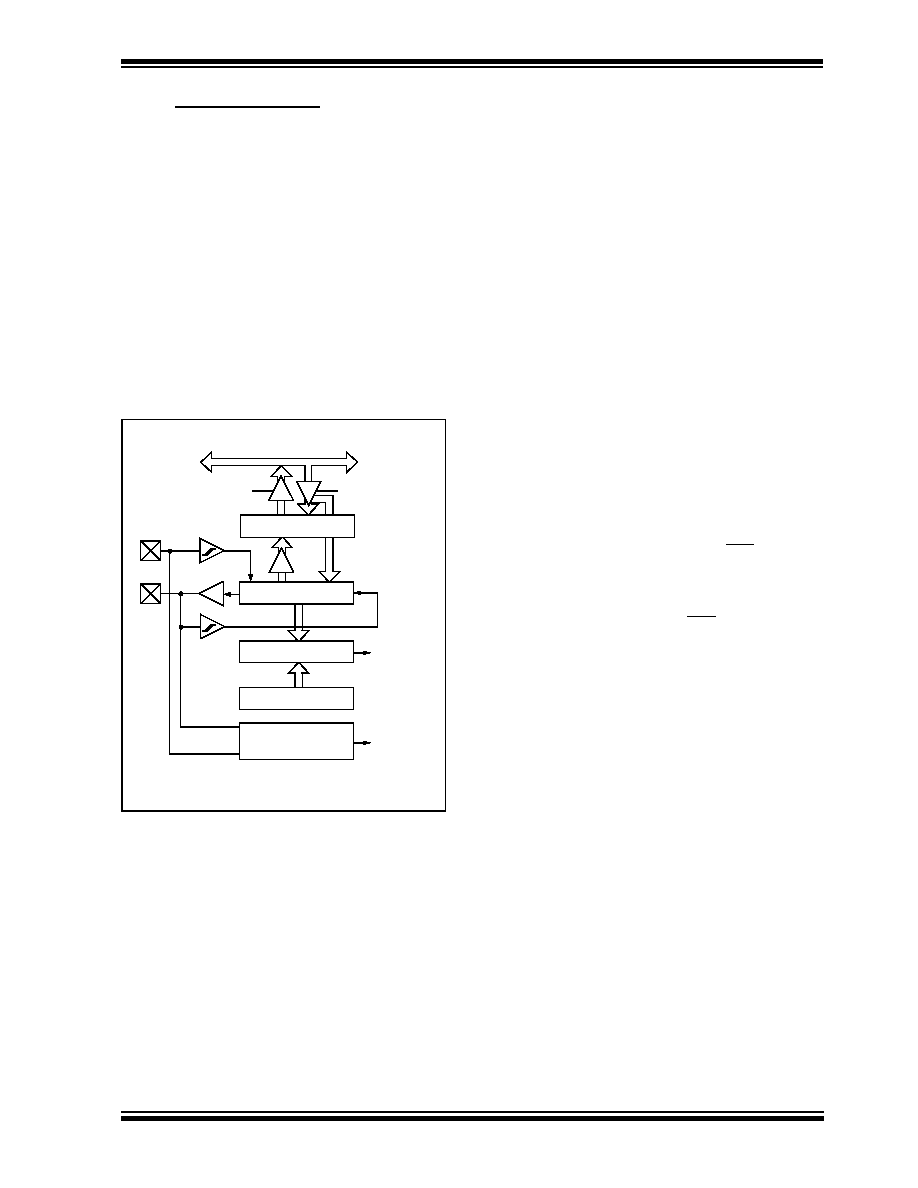
FIGURE 15-6: MSSP BLOCK DIAGRAM
(I2C MODE)
The MSSP module has these six registers for I2C oper-
ation:
MSSP Control Register1 (SSPCON1)
MSSP Control Register2 (SSPCON2)
MSSP Status Register (SSPSTAT)
Serial Receive/Transmit Buffer (SSPBUF)
MSSP Shift Register (SSPSR) - Not directly
accessible
MSSP Address Register (SSPADD)
The SSPCON1 register allows control of the I2C oper-
ation.
The
SSPM3:SSPM0
mode
selection
bits
(SSPCON1 register) allow one of the following I2C
modes to be selected:
I2C Master mode, clock = OSC/4 (SSPADD +1)
I2C Slave mode (7-bit address)
I2C Slave mode (10-bit address)
I2C Slave mode (7-bit address), with START and
STOP bit interrupts enabled
I2C Slave mode (10-bit address), with START and
STOP bit interrupts enabled
I2C Firmware controlled master operation, slave
is idle
Selection of any I2C mode with the SSPEN bit set,
forces the SCL and SDA pins to be open drain, pro-
vided these pins are programmed to inputs by setting
the appropriate TRISC bits.
15.4.1
SLAVE MODE
In Slave mode, the SCL and SDA pins must be config-
ured as inputs (TRISC<4:3> set). The MSSP module
will override the input state with the output data when
required (slave-transmitter).
When an address is matched, or the data transfer after
an address match is received, the hardware automati-
cally will generate the acknowledge (ACK) pulse and
load the SSPBUF register with the received value cur-
rently in the SSPSR register.
If either or both of the following conditions are true, the
MSSP module will not give this ACK pulse:
a)
The buffer full bit BF (SSPCON1 register) was
set before the transfer was received.
b)
The overflow bit SSPOV (SSPCON1 register)
was set before the transfer was received.
In this event, the SSPSR register value is not loaded
into the SSPBUF, but bit SSPIF (PIR registers) is set.
The BF bit is cleared by reading the SSPBUF register,
while bit SSPOV is cleared through software.
The SCL clock input must have a minimum high and
low for proper operation. The high and low times of the
I2C specification, as well as the requirement of the
MSSP module, is shown in timing parameter #100 and
parameter #101.
Read
Write
SSPSR reg
Match Detect
SSPADD reg
START and
STOP bit detect
SSPBUF reg
Internal
Data Bus
Addr Match
Set, RESET
S, P bits
(SSPSTAT reg)
RC3/SCK/SCL
RC4/
Shift
Clock
MSb
SDI/
LSb
SDA
Note:
I/O pins have diode protection to VDD and VSS.
相关PDF资料 |
PDF描述 |
|---|---|
| PIC18C858-I/PT | IC PIC MCU OTP 16KX16 80TQFP |
| PIC16F874-04E/P | IC MCU FLASH 4KX14 EE 40DIP |
| PIC18C442-E/P | IC MCU OTP 8KX16 A/D 40DIP |
| PIC16F874-04E/L | IC MCU FLASH 4KX14 EE 44PLCC |
| PIC16F874-10E/L | IC MCU FLASH 4KX14 EE 44PLCC |
相关代理商/技术参数 |
参数描述 |
|---|---|
| PIC18LC858T-I/L | 功能描述:8位微控制器 -MCU Low Power RoHS:否 制造商:Silicon Labs 核心:8051 处理器系列:C8051F39x 数据总线宽度:8 bit 最大时钟频率:50 MHz 程序存储器大小:16 KB 数据 RAM 大小:1 KB 片上 ADC:Yes 工作电源电压:1.8 V to 3.6 V 工作温度范围:- 40 C to + 105 C 封装 / 箱体:QFN-20 安装风格:SMD/SMT |
| PIC18LC858T-I/PT | 功能描述:8位微控制器 -MCU 32KB 1536 RAM 68I/O RoHS:否 制造商:Silicon Labs 核心:8051 处理器系列:C8051F39x 数据总线宽度:8 bit 最大时钟频率:50 MHz 程序存储器大小:16 KB 数据 RAM 大小:1 KB 片上 ADC:Yes 工作电源电压:1.8 V to 3.6 V 工作温度范围:- 40 C to + 105 C 封装 / 箱体:QFN-20 安装风格:SMD/SMT |
| PIC18LF1220-I/ML | 功能描述:8位微控制器 -MCU 4KB 256 RAM 16I/O RoHS:否 制造商:Silicon Labs 核心:8051 处理器系列:C8051F39x 数据总线宽度:8 bit 最大时钟频率:50 MHz 程序存储器大小:16 KB 数据 RAM 大小:1 KB 片上 ADC:Yes 工作电源电压:1.8 V to 3.6 V 工作温度范围:- 40 C to + 105 C 封装 / 箱体:QFN-20 安装风格:SMD/SMT |
| PIC18LF1220-I/P | 功能描述:8位微控制器 -MCU 4KB 256 RAM 16I/O RoHS:否 制造商:Silicon Labs 核心:8051 处理器系列:C8051F39x 数据总线宽度:8 bit 最大时钟频率:50 MHz 程序存储器大小:16 KB 数据 RAM 大小:1 KB 片上 ADC:Yes 工作电源电压:1.8 V to 3.6 V 工作温度范围:- 40 C to + 105 C 封装 / 箱体:QFN-20 安装风格:SMD/SMT |
| PIC18LF1220-I/SO | 功能描述:8位微控制器 -MCU 4KB 256 RAM 16I/O RoHS:否 制造商:Silicon Labs 核心:8051 处理器系列:C8051F39x 数据总线宽度:8 bit 最大时钟频率:50 MHz 程序存储器大小:16 KB 数据 RAM 大小:1 KB 片上 ADC:Yes 工作电源电压:1.8 V to 3.6 V 工作温度范围:- 40 C to + 105 C 封装 / 箱体:QFN-20 安装风格:SMD/SMT |
发布紧急采购,3分钟左右您将得到回复。