- 您现在的位置:买卖IC网 > PDF目录11471 > PIC24FJ48GA004-E/ML (Microchip Technology)IC PIC MCU FLASH 48K 44-QFN PDF资料下载
参数资料
| 型号: | PIC24FJ48GA004-E/ML |
| 厂商: | Microchip Technology |
| 文件页数: | 23/52页 |
| 文件大小: | 0K |
| 描述: | IC PIC MCU FLASH 48K 44-QFN |
| 特色产品: | PIC24FJ/33FJ MCUs & dsPIC? DSCs |
| 标准包装: | 45 |
| 系列: | PIC® 24F |
| 核心处理器: | PIC |
| 芯体尺寸: | 16-位 |
| 速度: | 32MHz |
| 连通性: | I²C,PMP,SPI,UART/USART |
| 外围设备: | 欠压检测/复位,LVD,POR,PWM,WDT |
| 输入/输出数: | 35 |
| 程序存储器容量: | 48KB(16K x 24) |
| 程序存储器类型: | 闪存 |
| RAM 容量: | 8K x 8 |
| 电压 - 电源 (Vcc/Vdd): | 2 V ~ 3.6 V |
| 数据转换器: | A/D 13x10b |
| 振荡器型: | 内部 |
| 工作温度: | -40°C ~ 125°C |
| 封装/外壳: | 44-VQFN 裸露焊盘 |
| 包装: | 管件 |
| 产品目录页面: | 647 (CN2011-ZH PDF) |
| 配用: | 876-1004-ND - PIC24 BREAKOUT BOARD DM240011-ND - KIT STARTER MPLAB FOR PIC24F MCU AC162088-ND - HEADER MPLAB ICD2 24FJ64GA004 28 AC164336-ND - MODULE SOCKET FOR PM3 28/44QFN DV164033-ND - KIT START EXPLORER 16 MPLAB ICD2 |
第1页第2页第3页第4页第5页第6页第7页第8页第9页第10页第11页第12页第13页第14页第15页第16页第17页第18页第19页第20页第21页第22页当前第23页第24页第25页第26页第27页第28页第29页第30页第31页第32页第33页第34页第35页第36页第37页第38页第39页第40页第41页第42页第43页第44页第45页第46页第47页第48页第49页第50页第51页第52页
2008 Microchip Technology Inc.
DS39768D-page 3
PIC24FJXXXGA0XX
2.2
Program Memory Write/Erase
Requirements
The Flash program memory on the PIC24FJXXXGA0XX
devices has a specific write/erase requirement that must
be adhered to for proper device operation. The rule is
that any given word in memory must not be written more
than twice before erasing the page in which it is located.
Thus, the easiest way to conform to this rule is to write
all the data in a programming block within one write
cycle. The programming methods specified in this
specification comply with this requirement.
2.3
Pin Diagrams
The pin diagrams for the PIC24FJXXXGA0XX family
are shown in the following figures. The pins that are
required for programming are listed in Table 2-1 and
are shown in bold letters in the figures. Refer to the
appropriate device data sheet for complete pin
descriptions.
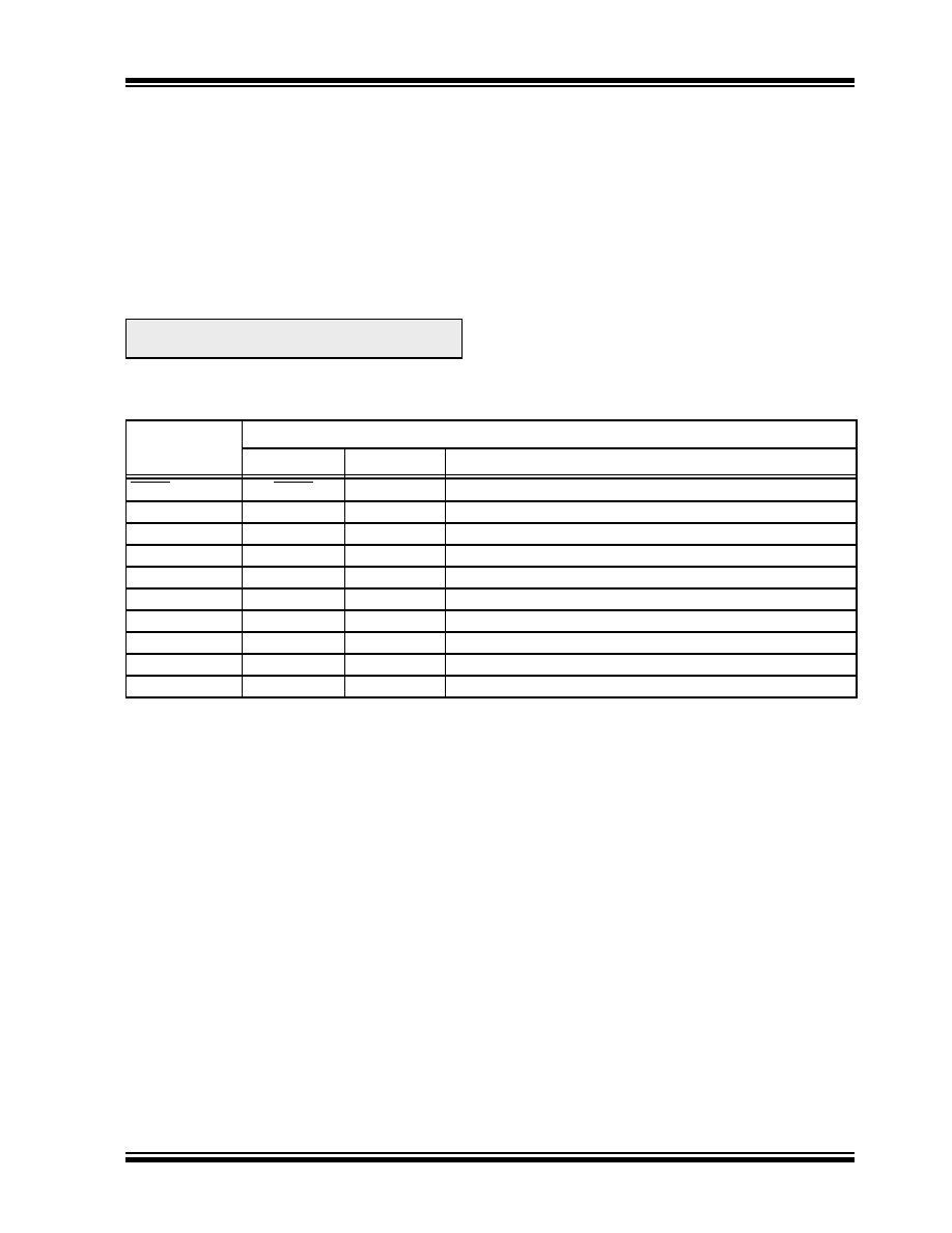
TABLE 2-1:
PIN DESCRIPTIONS (DURING PROGRAMMING)
Note:
Writing to a location multiple times without
erasing is not recommended.
Pin Name
During Programming
Pin Name
Pin Type
Pin Description
MCLR
P
Programming Enable
ENVREG
I
Enable for On-Chip Voltage Regulator
DISVREG(1)
DISVREG
I
Disable for On-Chip Voltage Regulator
VDD and AVDD(2)
VDD
P
Power Supply
VSS and AVSS(2)
VSS
PGround
VDDCORE
P
Regulated Power Supply for Core
PGC1
PGC
I
Primary Programming Pin Pair: Serial Clock
PGD1
PGD
I/O
Primary Programming Pin Pair: Serial Data
PGC2
PGC
I
Secondary Programming Pin Pair: Serial Clock
PGD2
PGD
I/O
Secondary Programming Pin Pair: Serial Data
Legend: I = Input, O = Output, P = Power
Note 1:
Applies to 28 and 44-pin devices only.
2:
All power supply and ground pins must be connected, including analog supplies (AVDD) and ground
(AVSS).
相关PDF资料 |
PDF描述 |
|---|---|
| PIC18F4221-E/P | IC PIC MCU FLASH 2KX16 40-DIP |
| DSPIC30F2012T-30I/ML | IC DSPIC MCU/DSP 12K 28QFN |
| DSPIC30F2011-20E/SO | IC DSPIC MCU/DSP 12K 18SOIC |
| DSPIC30F2012-20I/SP | IC DSPIC MCU/DSP 12K 28DIP |
| PIC18F1320-E/P | IC MCU FLASH 4KX16 EEPROM 18DIP |
相关代理商/技术参数 |
参数描述 |
|---|---|
| PIC24FJ48GA004-I/ML | 功能描述:16位微控制器 - MCU 48KB Flash 8192bytes RAM 35 I/O RoHS:否 制造商:Texas Instruments 核心:RISC 处理器系列:MSP430FR572x 数据总线宽度:16 bit 最大时钟频率:24 MHz 程序存储器大小:8 KB 数据 RAM 大小:1 KB 片上 ADC:Yes 工作电源电压:2 V to 3.6 V 工作温度范围:- 40 C to + 85 C 封装 / 箱体:VQFN-40 安装风格:SMD/SMT |
| PIC24FJ48GA004-I/PT | 功能描述:16位微控制器 - MCU 16b Fam 16 MIPS 48KB FL 8192b RAM 35 I/O RoHS:否 制造商:Texas Instruments 核心:RISC 处理器系列:MSP430FR572x 数据总线宽度:16 bit 最大时钟频率:24 MHz 程序存储器大小:8 KB 数据 RAM 大小:1 KB 片上 ADC:Yes 工作电源电压:2 V to 3.6 V 工作温度范围:- 40 C to + 85 C 封装 / 箱体:VQFN-40 安装风格:SMD/SMT |
| PIC24FJ48GA004T-I/ML | 功能描述:16位微控制器 - MCU 48KB Flash 8192bytes RAM 35 I/O RoHS:否 制造商:Texas Instruments 核心:RISC 处理器系列:MSP430FR572x 数据总线宽度:16 bit 最大时钟频率:24 MHz 程序存储器大小:8 KB 数据 RAM 大小:1 KB 片上 ADC:Yes 工作电源电压:2 V to 3.6 V 工作温度范围:- 40 C to + 85 C 封装 / 箱体:VQFN-40 安装风格:SMD/SMT |
| PIC24FJ48GA004T-I/PT | 功能描述:16位微控制器 - MCU 48KB Flash 8192bytes RAM 35 I/O RoHS:否 制造商:Texas Instruments 核心:RISC 处理器系列:MSP430FR572x 数据总线宽度:16 bit 最大时钟频率:24 MHz 程序存储器大小:8 KB 数据 RAM 大小:1 KB 片上 ADC:Yes 工作电源电压:2 V to 3.6 V 工作温度范围:- 40 C to + 85 C 封装 / 箱体:VQFN-40 安装风格:SMD/SMT |
| PIC24FJ64GA | 制造商:MICROCHIP 制造商全称:Microchip Technology 功能描述:28/44-Pin General Purpose, 16-Bit Flash Microcontrollers |
发布紧急采购,3分钟左右您将得到回复。