- 您现在的位置:买卖IC网 > PDF目录11471 > PIC24FJ48GA004-E/ML (Microchip Technology)IC PIC MCU FLASH 48K 44-QFN PDF资料下载
参数资料
| 型号: | PIC24FJ48GA004-E/ML |
| 厂商: | Microchip Technology |
| 文件页数: | 8/52页 |
| 文件大小: | 0K |
| 描述: | IC PIC MCU FLASH 48K 44-QFN |
| 特色产品: | PIC24FJ/33FJ MCUs & dsPIC? DSCs |
| 标准包装: | 45 |
| 系列: | PIC® 24F |
| 核心处理器: | PIC |
| 芯体尺寸: | 16-位 |
| 速度: | 32MHz |
| 连通性: | I²C,PMP,SPI,UART/USART |
| 外围设备: | 欠压检测/复位,LVD,POR,PWM,WDT |
| 输入/输出数: | 35 |
| 程序存储器容量: | 48KB(16K x 24) |
| 程序存储器类型: | 闪存 |
| RAM 容量: | 8K x 8 |
| 电压 - 电源 (Vcc/Vdd): | 2 V ~ 3.6 V |
| 数据转换器: | A/D 13x10b |
| 振荡器型: | 内部 |
| 工作温度: | -40°C ~ 125°C |
| 封装/外壳: | 44-VQFN 裸露焊盘 |
| 包装: | 管件 |
| 产品目录页面: | 647 (CN2011-ZH PDF) |
| 配用: | 876-1004-ND - PIC24 BREAKOUT BOARD DM240011-ND - KIT STARTER MPLAB FOR PIC24F MCU AC162088-ND - HEADER MPLAB ICD2 24FJ64GA004 28 AC164336-ND - MODULE SOCKET FOR PM3 28/44QFN DV164033-ND - KIT START EXPLORER 16 MPLAB ICD2 |
第1页第2页第3页第4页第5页第6页第7页当前第8页第9页第10页第11页第12页第13页第14页第15页第16页第17页第18页第19页第20页第21页第22页第23页第24页第25页第26页第27页第28页第29页第30页第31页第32页第33页第34页第35页第36页第37页第38页第39页第40页第41页第42页第43页第44页第45页第46页第47页第48页第49页第50页第51页第52页
PIC24FJXXXGA0XX
DS39768D-page 16
2008 Microchip Technology Inc.
3.4
Flash Memory Programming in
ICSP Mode
3.4.1
PROGRAMMING OPERATIONS
Flash memory write and erase operations are controlled
by the NVMCON register. Programming is performed by
setting NVMCON to select the type of erase operation
(Table 3-2) or write operation (Table 3-3) and initiating
the programming by setting the WR control bit
(NVMCON<15>).
In ICSP mode, all programming operations are
self-timed. There is an internal delay between the user
setting the WR control bit and the automatic clearing of
the WR control bit when the programming operation
is complete. Please refer to Section 7.0 “AC/DC
information about the delays associated with various
programming operations.
TABLE 3-2:
NVMCON ERASE
OPERATIONS
TABLE 3-3:
NVMCON WRITE
OPERATIONS
3.4.2
STARTING AND STOPPING A
PROGRAMMING CYCLE
The WR bit (NVMCON<15>) is used to start an erase or
write cycle. Setting the WR bit initiates the programming
cycle.
All erase and write cycles are self-timed. The WR bit
should be polled to determine if the erase or write cycle
has been completed. Starting a programming cycle is
performed as follows:
3.5
Erasing Program Memory
The procedure for erasing program memory (all of code
memory,
data
memory,
executive
memory
and
code-protect bits) consists of setting NVMCON to
404Fh and executing the programming cycle.
A Chip Erase can erase all of user memory or all of both
the user and configuration memory. A table write
instruction should be executed prior to performing the
Chip Erase to select which sections are erased.
When this table write instruction is executed:
If the TBLPAG register points to user space (is
less than 0x80), the Chip Erase will erase only
user memory.
If TBLPAG points to configuration space (is
greater than or equal to 0x80), the Chip Erase will
erase both user and configuration memory.
If configuration memory is erased, the internal
oscillator Calibration Word, located at 0x807FE,
will be erased. This location should be stored prior
to performing a whole Chip Erase and restored
afterward to prevent internal oscillators from
becoming uncalibrated.
Figure 3-5 shows the ICSP programming process for
performing a Chip Erase. This process includes the
ICSP command code, which must be transmitted (for
each instruction), Least Significant bit first, using the
PGCx and PGDx pins (see Figure 3-2).
FIGURE 3-5:
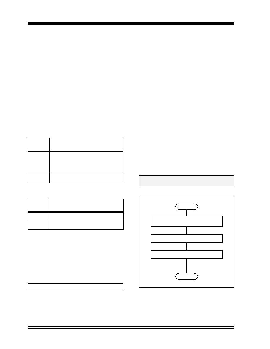
CHIP ERASE FLOW
NVMCON
Value
Erase Operation
404Fh
Erase all code memory, executive
memory and Configuration registers
(does not erase Unit ID or Device ID
registers).
4042h
Erase a page of code memory or
executive memory.
NVMCON
Value
Write Operation
4003h
Write a Configuration Word register.
4001h
Program 1 row (64 instruction words) of
code memory or executive memory.
BSET
NVMCON, #WR
Note:
Program memory must be erased before
writing any data to program memory.
Start
Done
Set the WR bit to Initiate Erase
Write 404Fh to NVMCON SFR
Delay P11 + P10 Time
相关PDF资料 |
PDF描述 |
|---|---|
| PIC18F4221-E/P | IC PIC MCU FLASH 2KX16 40-DIP |
| DSPIC30F2012T-30I/ML | IC DSPIC MCU/DSP 12K 28QFN |
| DSPIC30F2011-20E/SO | IC DSPIC MCU/DSP 12K 18SOIC |
| DSPIC30F2012-20I/SP | IC DSPIC MCU/DSP 12K 28DIP |
| PIC18F1320-E/P | IC MCU FLASH 4KX16 EEPROM 18DIP |
相关代理商/技术参数 |
参数描述 |
|---|---|
| PIC24FJ48GA004-I/ML | 功能描述:16位微控制器 - MCU 48KB Flash 8192bytes RAM 35 I/O RoHS:否 制造商:Texas Instruments 核心:RISC 处理器系列:MSP430FR572x 数据总线宽度:16 bit 最大时钟频率:24 MHz 程序存储器大小:8 KB 数据 RAM 大小:1 KB 片上 ADC:Yes 工作电源电压:2 V to 3.6 V 工作温度范围:- 40 C to + 85 C 封装 / 箱体:VQFN-40 安装风格:SMD/SMT |
| PIC24FJ48GA004-I/PT | 功能描述:16位微控制器 - MCU 16b Fam 16 MIPS 48KB FL 8192b RAM 35 I/O RoHS:否 制造商:Texas Instruments 核心:RISC 处理器系列:MSP430FR572x 数据总线宽度:16 bit 最大时钟频率:24 MHz 程序存储器大小:8 KB 数据 RAM 大小:1 KB 片上 ADC:Yes 工作电源电压:2 V to 3.6 V 工作温度范围:- 40 C to + 85 C 封装 / 箱体:VQFN-40 安装风格:SMD/SMT |
| PIC24FJ48GA004T-I/ML | 功能描述:16位微控制器 - MCU 48KB Flash 8192bytes RAM 35 I/O RoHS:否 制造商:Texas Instruments 核心:RISC 处理器系列:MSP430FR572x 数据总线宽度:16 bit 最大时钟频率:24 MHz 程序存储器大小:8 KB 数据 RAM 大小:1 KB 片上 ADC:Yes 工作电源电压:2 V to 3.6 V 工作温度范围:- 40 C to + 85 C 封装 / 箱体:VQFN-40 安装风格:SMD/SMT |
| PIC24FJ48GA004T-I/PT | 功能描述:16位微控制器 - MCU 48KB Flash 8192bytes RAM 35 I/O RoHS:否 制造商:Texas Instruments 核心:RISC 处理器系列:MSP430FR572x 数据总线宽度:16 bit 最大时钟频率:24 MHz 程序存储器大小:8 KB 数据 RAM 大小:1 KB 片上 ADC:Yes 工作电源电压:2 V to 3.6 V 工作温度范围:- 40 C to + 85 C 封装 / 箱体:VQFN-40 安装风格:SMD/SMT |
| PIC24FJ64GA | 制造商:MICROCHIP 制造商全称:Microchip Technology 功能描述:28/44-Pin General Purpose, 16-Bit Flash Microcontrollers |
发布紧急采购,3分钟左右您将得到回复。