- 您现在的位置:买卖IC网 > PDF目录11471 > PIC24FJ48GA004-E/ML (Microchip Technology)IC PIC MCU FLASH 48K 44-QFN PDF资料下载
参数资料
| 型号: | PIC24FJ48GA004-E/ML |
| 厂商: | Microchip Technology |
| 文件页数: | 5/52页 |
| 文件大小: | 0K |
| 描述: | IC PIC MCU FLASH 48K 44-QFN |
| 特色产品: | PIC24FJ/33FJ MCUs & dsPIC? DSCs |
| 标准包装: | 45 |
| 系列: | PIC® 24F |
| 核心处理器: | PIC |
| 芯体尺寸: | 16-位 |
| 速度: | 32MHz |
| 连通性: | I²C,PMP,SPI,UART/USART |
| 外围设备: | 欠压检测/复位,LVD,POR,PWM,WDT |
| 输入/输出数: | 35 |
| 程序存储器容量: | 48KB(16K x 24) |
| 程序存储器类型: | 闪存 |
| RAM 容量: | 8K x 8 |
| 电压 - 电源 (Vcc/Vdd): | 2 V ~ 3.6 V |
| 数据转换器: | A/D 13x10b |
| 振荡器型: | 内部 |
| 工作温度: | -40°C ~ 125°C |
| 封装/外壳: | 44-VQFN 裸露焊盘 |
| 包装: | 管件 |
| 产品目录页面: | 647 (CN2011-ZH PDF) |
| 配用: | 876-1004-ND - PIC24 BREAKOUT BOARD DM240011-ND - KIT STARTER MPLAB FOR PIC24F MCU AC162088-ND - HEADER MPLAB ICD2 24FJ64GA004 28 AC164336-ND - MODULE SOCKET FOR PM3 28/44QFN DV164033-ND - KIT START EXPLORER 16 MPLAB ICD2 |
第1页第2页第3页第4页当前第5页第6页第7页第8页第9页第10页第11页第12页第13页第14页第15页第16页第17页第18页第19页第20页第21页第22页第23页第24页第25页第26页第27页第28页第29页第30页第31页第32页第33页第34页第35页第36页第37页第38页第39页第40页第41页第42页第43页第44页第45页第46页第47页第48页第49页第50页第51页第52页
2008 Microchip Technology Inc.
DS39768D-page 13
PIC24FJXXXGA0XX
3.2.1
SIX SERIAL INSTRUCTION
EXECUTION
The SIX
control
code allows
execution of
the
PIC24FJXXXGA0XX
family
assembly
instructions.
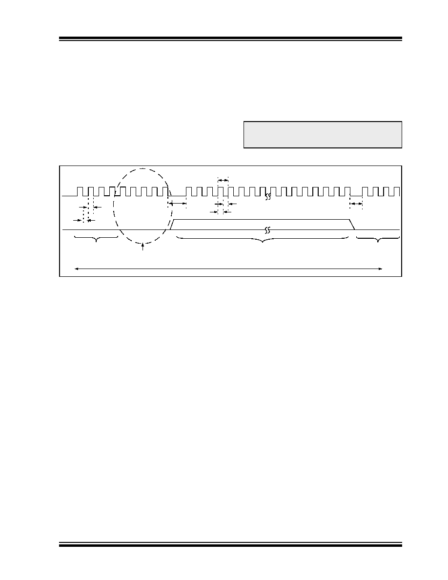
When the SIX code is received, the CPU is suspended
for 24 clock cycles, as the instruction is then clocked into
the internal buffer. Once the instruction is shifted in, the
state machine allows it to be executed over the next four
PGC clock cycles. While the received instruction is
executed, the state machine simultaneously shifts in the
next 4-bit command (see Figure 3-2).
Coming out of Reset, the first 4-bit control code is
always forced to SIX and a forced NOP instruction is
executed by the CPU. Five additional PGCx clocks are
needed on start-up, resulting in a 9-bit SIX command
instead of the normal 4-bit SIX command.
After the forced SIX is clocked in, ICSP operation
resumes as normal. That is, the next 24 clock cycles
load the first instruction word to the CPU.
FIGURE 3-2:
SIX SERIAL EXECUTION
3.2.1.1
Differences Between Execution of
SIX and Normal Instructions
There are some differences between executing instruc-
tions normally and using the SIX ICSP command. As a
result, the code examples in this specification may not
match those for performing the same functions during
normal device operation.
The important differences are:
Two-word instructions require two SIX operations
to clock in all the necessary data.
Examples of two-word instructions are GOTO and
CALL
.
Two-cycle instructions require two SIX operations.
The first SIX operation shifts in the instruction and
begins to execute it. A second SIX operation – which
should shift in a NOP to avoid losing data – provides
the CPU clocks required to finish executing the
instruction.
Examples of two-cycle instructions are table read
and table write instructions.
The CPU does not automatically stall to account
for pipeline changes.
A CPU stall occurs when an instruction modifies a
register that is used for Indirect Addressing by the
following instruction.
During normal operation, the CPU automatically
will force a NOP while the new data is read. When
using ICSP, there is no automatic stall, so any
indirect
references
to
a
recently
modified
register should be preceded by a NOP.
For example, the instructions, mov #0x0,W0 and
mov [W0],W1
,
must
have
a
NOP
inserted
between them.
If a two-cycle instruction modifies a register that is
used indirectly, it will require two following NOPs: one
to execute the second half of the instruction and a
second to stall the CPU to correct the pipeline.
Instructions
such
as
tblwtl [W0++],[W1]
should be followed by two NOPs.
The device Program Counter (PC) continues to
automatically increment during ICSP instruction
execution, even though the Flash memory is not
being used.
As a result, the PC may be incremented to point to
invalid memory locations. Invalid memory spaces
include unimplemented Flash addresses and the
vector space (locations 0x0 to 0x1FF).
If the PC points to these locations, the device will
reset, possibly interrupting the ICSP operation. To
prevent this, instructions should be periodically
executed to reset the PC to a safe space. The
optimal method to accomplish this is to perform a
GOTO 0x200
.
Note:
To account for this forced NOP, all example
code in this specification begin with a NOP
to ensure that no data is lost.
P4
23
1
2
3
23
24
1
2
3
4
P1
PGCx
P4A
PGDx
24-Bit Instruction Fetch
Execute PC – 1,
16
00
0
Fetch SIX
45
6
7
8
18
19
20
21
22
17
LSB X
X
X MSB
PGDx = Input
P2
P3
P1B
P1A
78
9
00
0
00
0
Only for
Program
Memory Entry
Control Code
4
5
Execute 24-Bit
Instruction, Fetch
Next Control Code
00
相关PDF资料 |
PDF描述 |
|---|---|
| PIC18F4221-E/P | IC PIC MCU FLASH 2KX16 40-DIP |
| DSPIC30F2012T-30I/ML | IC DSPIC MCU/DSP 12K 28QFN |
| DSPIC30F2011-20E/SO | IC DSPIC MCU/DSP 12K 18SOIC |
| DSPIC30F2012-20I/SP | IC DSPIC MCU/DSP 12K 28DIP |
| PIC18F1320-E/P | IC MCU FLASH 4KX16 EEPROM 18DIP |
相关代理商/技术参数 |
参数描述 |
|---|---|
| PIC24FJ48GA004-I/ML | 功能描述:16位微控制器 - MCU 48KB Flash 8192bytes RAM 35 I/O RoHS:否 制造商:Texas Instruments 核心:RISC 处理器系列:MSP430FR572x 数据总线宽度:16 bit 最大时钟频率:24 MHz 程序存储器大小:8 KB 数据 RAM 大小:1 KB 片上 ADC:Yes 工作电源电压:2 V to 3.6 V 工作温度范围:- 40 C to + 85 C 封装 / 箱体:VQFN-40 安装风格:SMD/SMT |
| PIC24FJ48GA004-I/PT | 功能描述:16位微控制器 - MCU 16b Fam 16 MIPS 48KB FL 8192b RAM 35 I/O RoHS:否 制造商:Texas Instruments 核心:RISC 处理器系列:MSP430FR572x 数据总线宽度:16 bit 最大时钟频率:24 MHz 程序存储器大小:8 KB 数据 RAM 大小:1 KB 片上 ADC:Yes 工作电源电压:2 V to 3.6 V 工作温度范围:- 40 C to + 85 C 封装 / 箱体:VQFN-40 安装风格:SMD/SMT |
| PIC24FJ48GA004T-I/ML | 功能描述:16位微控制器 - MCU 48KB Flash 8192bytes RAM 35 I/O RoHS:否 制造商:Texas Instruments 核心:RISC 处理器系列:MSP430FR572x 数据总线宽度:16 bit 最大时钟频率:24 MHz 程序存储器大小:8 KB 数据 RAM 大小:1 KB 片上 ADC:Yes 工作电源电压:2 V to 3.6 V 工作温度范围:- 40 C to + 85 C 封装 / 箱体:VQFN-40 安装风格:SMD/SMT |
| PIC24FJ48GA004T-I/PT | 功能描述:16位微控制器 - MCU 48KB Flash 8192bytes RAM 35 I/O RoHS:否 制造商:Texas Instruments 核心:RISC 处理器系列:MSP430FR572x 数据总线宽度:16 bit 最大时钟频率:24 MHz 程序存储器大小:8 KB 数据 RAM 大小:1 KB 片上 ADC:Yes 工作电源电压:2 V to 3.6 V 工作温度范围:- 40 C to + 85 C 封装 / 箱体:VQFN-40 安装风格:SMD/SMT |
| PIC24FJ64GA | 制造商:MICROCHIP 制造商全称:Microchip Technology 功能描述:28/44-Pin General Purpose, 16-Bit Flash Microcontrollers |
发布紧急采购,3分钟左右您将得到回复。