- 您现在的位置:买卖IC网 > PDF目录11254 > PIC32MX575F256L-80I/BG (Microchip Technology)IC MCU 32BIT 256KB FLASH 121XBGA PDF资料下载
参数资料
| 型号: | PIC32MX575F256L-80I/BG |
| 厂商: | Microchip Technology |
| 文件页数: | 20/64页 |
| 文件大小: | 0K |
| 描述: | IC MCU 32BIT 256KB FLASH 121XBGA |
| 特色产品: | 32-Bit PIC? Microcontroller PIC32 32-Bit MCU Families |
| 标准包装: | 184 |
| 系列: | PIC® 32MX |
| 核心处理器: | MIPS32? M4K? |
| 芯体尺寸: | 32-位 |
| 速度: | 80MHz |
| 连通性: | CAN,I²C,SPI,UART/USART,USB OTG |
| 外围设备: | 欠压检测/复位,DMA,POR,PWM,WDT |
| 程序存储器容量: | 256KB(256K x 8) |
| 程序存储器类型: | 闪存 |
| RAM 容量: | 64K x 8 |
| 电压 - 电源 (Vcc/Vdd): | 2.3 V ~ 3.6 V |
| 数据转换器: | A/D 16x10b |
| 振荡器型: | 内部 |
| 工作温度: | -40°C ~ 85°C |
| 封装/外壳: | 121-TFBGA |
| 包装: | 托盘 |
| 产品目录页面: | 650 (CN2011-ZH PDF) |
第1页第2页第3页第4页第5页第6页第7页第8页第9页第10页第11页第12页第13页第14页第15页第16页第17页第18页第19页当前第20页第21页第22页第23页第24页第25页第26页第27页第28页第29页第30页第31页第32页第33页第34页第35页第36页第37页第38页第39页第40页第41页第42页第43页第44页第45页第46页第47页第48页第49页第50页第51页第52页第53页第54页第55页第56页第57页第58页第59页第60页第61页第62页第63页第64页
2007-2012 Microchip Technology Inc.
DS61145K-page 27
PIC32MX
13.0
INITIATING A FLASH ROW
WRITE
Once a row of data has been downloaded into the
device’s SRAM, the programming sequence must be
initiated to write the block of data to Flash memory.
13.1
With the PE
When using the PE, the data is immediately written to
the Flash memory from the SRAM. No further action is
required.
13.2
Without the PE
Flash memory write operations are controlled by the
NVMCON register. Programming is performed by set-
ting NVMCON to select the type of write operation and
initiating the programming sequence by setting the WR
control bit (NVMCON<15>).
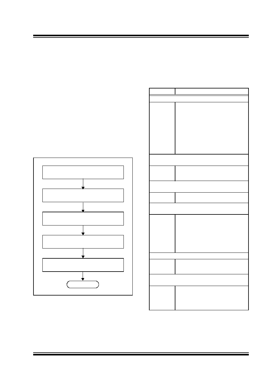
FIGURE 13-1:
INITIATING FLASH WRITE
WITHOUT THE PE
The following steps are required to initiate a Flash
write:
1.
XferInstruction
(op code).
2.
Repeat Step 1 until the last instruction is
transferred to the CPU.
Start Operation
Unlock Flash Controller
Load Addresses in NVM Registers
Select Write Operation
Unprotect Control Registers
Done
TABLE 13-1:
INITIATE FLASH ROW WRITE
OP CODES
Op code
Instruction
Step 1: Initialize some constants.
3c04bf80
3484f400
34054003
34068000
34074000
3c11aa99
36316655
3c125566
365299aa
3c13ff20
3c100000
lui a0,0xbf80
ori a0,a0,0xf400
ori a1,$0,0x4003
ori a2,$0,0x8000
ori a3,$0,0x4000
lui s1,0xaa99
ori s1,s1,0x6655
lui s2,0x5566
ori s2,s2,0x99aa
lui s3,0xff20
lui s0,0x0000
Step 2: Set NVMADDR with the address of the
Flash row to be programmed.
3c08<ADDR>
3508<ADDR>
ac880020
lui t0,<FLASH_ROW_ADDR(31:16)>
ori t0,t0,<FLASH_ROW_ADDR(15:0)>
sw
t0,32(a0)
Step 3: Set NVMSRCADDR with the physical
source SRAM address.
3610<ADDR>
ac900040
ori s0,s0,<RAM_ADDR(15:0)>
sw
s0,64(a0)
Step 4: Set up NVMCON for write operation and poll
LVDSTAT.
ac850000
8C880000
31080800
1500fffd
00000000
sw
a1,0(a0)
delay (6 s)
here1:
lw
t0,0(a0)
andit0,t0,0x0800
bne t0,$0,<here1>
nop
Step 5: Unlock NVMCON and start write operation.
ac910010
ac920010
ac860008
sw
s1,16(a0)
sw
s2,16(a0)
sw
a2,8(a0)
Step 6: Repeatedly read the NVMCON register and
poll for WR bit to get cleared.
8c880000
01064024
1500fffd
00000000
here2:
lw
t0,0(a0)
and t0,t0,a2
bne t0,$0,<here2>
nop
相关PDF资料 |
PDF描述 |
|---|---|
| VI-2VN-IX-F1 | CONVERTER MOD DC/DC 18.5V 75W |
| PIC17C44-16/PT | IC MCU OTP 8KX16 PWM 44TQFP |
| PIC17C44-16/PQ | IC MCU OTP 8KX16 PWM 44-MQFP |
| VI-2VM-IX-F3 | CONVERTER MOD DC/DC 10V 75W |
| ADG719BRT-REEL7 | IC SWITCH SPDT SOT23-6 |
相关代理商/技术参数 |
参数描述 |
|---|---|
| PIC32MX575F256L-80IPF | 制造商:MICROCHIP 制造商全称:Microchip Technology 功能描述:PIC32MX575FXXXX USB, CAN and Ethernet 32-bit Flash Microcontroller |
| PIC32MX575F256L-80IPT | 制造商:MICROCHIP 制造商全称:Microchip Technology 功能描述:PIC32MX575FXXXX USB, CAN and Ethernet 32-bit Flash Microcontroller |
| PIC32MX575F256L-80V/BG | 功能描述:32位微控制器 - MCU 256KB 64KBRM USB-OTG CAN 80MHz 10BIT RoHS:否 制造商:Texas Instruments 核心:C28x 处理器系列:TMS320F28x 数据总线宽度:32 bit 最大时钟频率:90 MHz 程序存储器大小:64 KB 数据 RAM 大小:26 KB 片上 ADC:Yes 工作电源电压:2.97 V to 3.63 V 工作温度范围:- 40 C to + 105 C 封装 / 箱体:LQFP-80 安装风格:SMD/SMT |
| PIC32MX575F256L-80V/PF | 功能描述:32位微控制器 - MCU 256KB 64KBRM USB-OTG CAN 80MHz 10BIT RoHS:否 制造商:Texas Instruments 核心:C28x 处理器系列:TMS320F28x 数据总线宽度:32 bit 最大时钟频率:90 MHz 程序存储器大小:64 KB 数据 RAM 大小:26 KB 片上 ADC:Yes 工作电源电压:2.97 V to 3.63 V 工作温度范围:- 40 C to + 105 C 封装 / 箱体:LQFP-80 安装风格:SMD/SMT |
| PIC32MX575F256L-80V/PT | 功能描述:32位微控制器 - MCU 256KB 64KBRM USB-OTG CAN 80MHz 10BIT RoHS:否 制造商:Texas Instruments 核心:C28x 处理器系列:TMS320F28x 数据总线宽度:32 bit 最大时钟频率:90 MHz 程序存储器大小:64 KB 数据 RAM 大小:26 KB 片上 ADC:Yes 工作电源电压:2.97 V to 3.63 V 工作温度范围:- 40 C to + 105 C 封装 / 箱体:LQFP-80 安装风格:SMD/SMT |
发布紧急采购,3分钟左右您将得到回复。