参数资料
| 型号: | PPC5604BCLL64 |
| 厂商: | Freescale Semiconductor |
| 文件页数: | 58/109页 |
| 文件大小: | 0K |
| 描述: | MCU 32BIT 512K 64MHZ |
| 标准包装: | 90 |
| 系列: | MPC56xx Qorivva |
| 核心处理器: | e200z0h |
| 芯体尺寸: | 32-位 |
| 速度: | 64MHz |
| 连通性: | CAN,I²C,LIN,SCI,SPI |
| 外围设备: | POR,PWM,WDT |
| 输入/输出数: | 79 |
| 程序存储器容量: | 512KB(512K x 8) |
| 程序存储器类型: | 闪存 |
| EEPROM 大小: | 4K x 16 |
| RAM 容量: | 32K x 8 |
| 电压 - 电源 (Vcc/Vdd): | 3 V ~ 3.6 V |
| 数据转换器: | A/D 28x10b |
| 振荡器型: | 内部 |
| 工作温度: | -40°C ~ 85°C |
| 封装/外壳: | 100-LQFP |
| 包装: | 托盘 |
第1页第2页第3页第4页第5页第6页第7页第8页第9页第10页第11页第12页第13页第14页第15页第16页第17页第18页第19页第20页第21页第22页第23页第24页第25页第26页第27页第28页第29页第30页第31页第32页第33页第34页第35页第36页第37页第38页第39页第40页第41页第42页第43页第44页第45页第46页第47页第48页第49页第50页第51页第52页第53页第54页第55页第56页第57页当前第58页第59页第60页第61页第62页第63页第64页第65页第66页第67页第68页第69页第70页第71页第72页第73页第74页第75页第76页第77页第78页第79页第80页第81页第82页第83页第84页第85页第86页第87页第88页第89页第90页第91页第92页第93页第94页第95页第96页第97页第98页第99页第100页第101页第102页第103页第104页第105页第106页第107页第108页第109页
MPC5604B/C Microcontroller Data Sheet, Rev. 11.1
Package pinouts and signal descriptions
Freescale Semiconductor
52
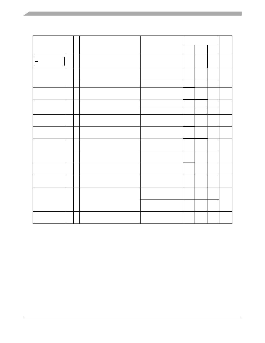
The
VDD(STDBY)| and dVDD(STDBY)/dt system requirement can be used to define the component used for the VDD supply
generation. The following two examples describe how to calculate capacitance size:
SR — Maximum slope on VDD during
standby exit
——
15
mV/s
VMREG
CC T Main regulator output voltage
Before exiting from
reset
—
1.32
—
V
P
After trimming
1.16
1.28
—
IMREG
SR — Main regulator current provided to
VDD_LV domain
——
—
150
mA
IMREGINT
CC D Main regulator module current
consumption
IMREG = 200 mA
—
2
mA
IMREG = 0 mA
—
1
VLPREG
CC P Low power regulator output
voltage
After trimming
1.16
1.28
—
V
ILPREG
SR — Low power regulator current
provided to VDD_LV domain
—
——
15
mA
ILPREGINT
CC D Low power regulator module
current consumption
ILPREG = 15 mA;
TA = 55 °C
——
600
A
—
ILPREG = 0 mA;
TA = 55 °C
—
5—
VULPREG
CC P Ultra low power regulator output
voltage
After trimming
1.16
1.28
—
V
IULPREG
SR — Ultra low power regulator current
provided to VDD_LV domain
——
—
5
mA
IULPREGINT
CC D Ultra low power regulator module
current consumption
IULPREG = 5 mA;
TA = 55 °C
——
100
A
IULPREG = 0 mA;
TA = 55 °C
—
2—
IDD_BV
CC D In-rush average current on VDD_BV
during power-up5
——
—
3006
mA
1 VDD = 3.3 V ± 10% / 5.0 V ± 10%, TA = 40 to 125 °C, unless otherwise specified
2 This capacitance value is driven by the constraints of the external voltage regulator supplying the VDD_BV voltage.
A typical value is in the range of 470 nF.
3 This value is acceptable to guarantee operation from 4.5 V to 5.5 V
4 External regulator and capacitance circuitry must be capable of providing IDD_BV while maintaining supply VDD_BV
in operating range.
5 In-rush average current is seen only for short time (maximum 20 s) during power-up and on standby exit. It is
dependant on the sum of the CREGn capacitances.
6 The duration of the in-rush current depends on the capacitance placed on LV pins. BV decoupling capacitors must
be sized accordingly. Refer to IMREG value for minimum amount of current to be provided in cc.
Table 25. Voltage regulator electrical characteristics (continued)
Symbol
C
Parameter
Conditions1
Value
Unit
Min
Typ
Max
t
d
d VDD STDBY
相关PDF资料 |
PDF描述 |
|---|---|
| PPC5606BCLU64 | MCU 32BIT 1M 64MHZ |
| PPC8309VMAGDCA | MPU POWERQUICC II PRO 489-MAP |
| PS302CSA | IC SWITCH SPST 8SOIC |
| PS321CPA | IC SWITCH DUAL SPST 8DIP |
| PS323CUAEX | IC ANLG SW SPST DUAL NO 8-MSOP |
相关代理商/技术参数 |
参数描述 |
|---|---|
| PPC5604BCLQ64 | 制造商:Freescale Semiconductor 功能描述:BOL 512K 3 CAN 64MHZ - Bulk |
| PPC5604BECLQ | 制造商:FREESCALE 制造商全称:Freescale Semiconductor, Inc 功能描述:Microcontroller |
| PPC5604BECLU | 制造商:FREESCALE 制造商全称:Freescale Semiconductor, Inc 功能描述:Microcontroller |
| PPC5604BECMG | 制造商:FREESCALE 制造商全称:Freescale Semiconductor, Inc 功能描述:Microcontroller |
| PPC5604BEF1MLL | 制造商:Freescale Semiconductor 功能描述: |
发布紧急采购,3分钟左右您将得到回复。